4-Layer Heavy Copper PCB Design Guide: Enhance Thermal Performance in Power Electronics

Ruiheng PCB
2026-02-25
Tutorial Guide
Is your industrial power supply PCB prone to overheating? This 4-layer heavy copper PCB design guide reveals key solutions:提升 heat dissipation efficiency and current carrying capacity through optimal 4oz copper thickness selection. Combined with high Tg FR-4 material (170°C) and ENIG surface finish, achieve stable operation in harsh environments. The guide delves into stack-up configuration, line spacing control (minimum 0.3mm), impedance matching, and thick copper etching challenges. It includes a practical design checklist and real application cases to help you optimize power electronic system performance and avoid common pitfalls.
https://shmuker.oss-accelerate.aliyuncs.com/data/oss/20251230/76402db4ddda640df1d8ea772a31c807/0ec0487d-c513-4ae1-bddb-49f7de806bce.jpeg

Power electronics engineers know the frustration: you've designed a compact power supply, tested it in the lab, only to find it overheats in real-world conditions. The root cause often lies not in component selection, but in a foundational element you might be overlooking—your PCB design, specifically copper thickness. Let's explore how upgrading to 4-layer thick copper PCBs can transform your thermal management strategy and reliability outcomes.

The Thermal Challenge in Modern Power Electronics

Consider this: a standard 1oz copper PCB conducting 10A current will experience a temperature rise of approximately 45°C over ambient conditions. In contrast, a 4oz copper design under the same load shows a temperature increase of just 12°C—a 73% reduction in thermal rise. This isn't just a numbers game; it directly translates to reliability. Field data shows that every 10°C reduction in operating temperature can double the lifespan of power electronics components.

Designer's Dilemma: When Standard PCBs Fail

Many engineers face this scenario: your design meets all electrical specifications on paper, but in the field, thermal issues emerge. Common warning signs include:

  • Component degradation within expected service life
  • Erratic performance under load variations
  • Reduced efficiency at operating temperatures above 50°C
  • Failure to meet thermal certification requirements

Copper Thickness: The Unsung Hero of Thermal Management

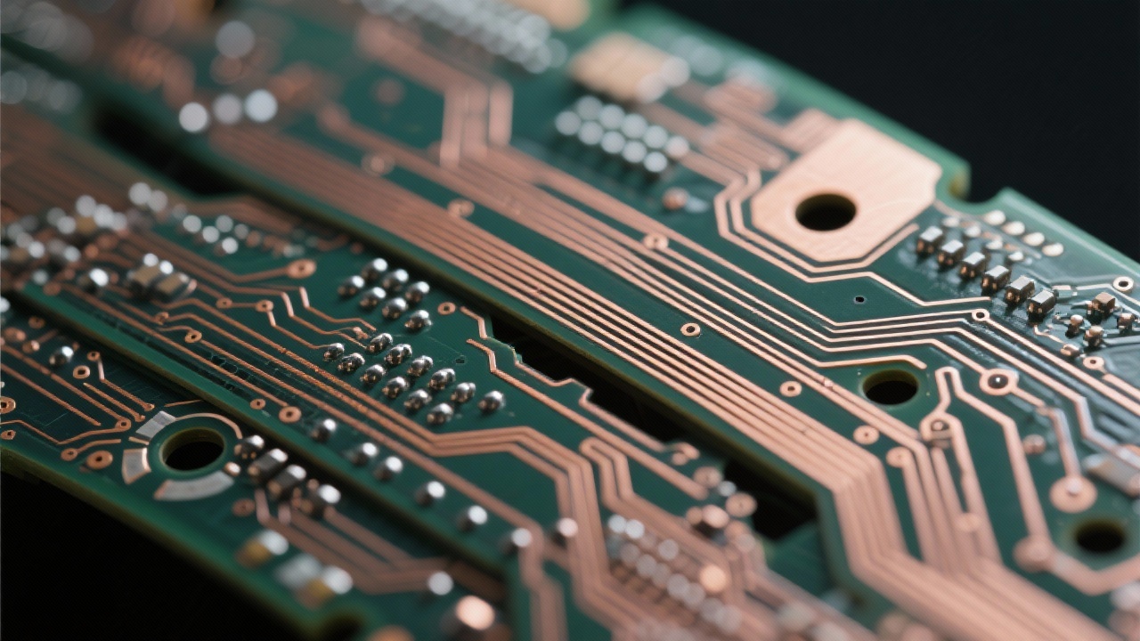
Copper serves dual roles in power PCBs—as both electrical conductor and heat dissipator. The correlation between copper thickness and thermal performance is exponential rather than linear. While 1oz copper (35μm) is standard for most applications, stepping up to 4oz (140μm) provides:

Enhanced Current Carrying Capacity

A 4oz copper trace can carry 2.8 times more current than an equivalent width 1oz trace without exceeding temperature limits, reducing the need for large, space-consuming traces.

Superior Heat Spreading

Thicker copper creates a thermal highway that distributes heat more evenly across the board, preventing hotspots around critical components like MOSFETs and diodes.

Temperature rise comparison between 1oz and 4oz copper PCBs under various current loads

Material Selection: Beyond Copper Thickness

While copper thickness is critical, material selection completes the thermal management equation. High Tg FR-4 material (Tg=170°C) maintains mechanical stability at operating temperatures 30-40°C higher than standard FR-4 (Tg=130-140°C). This becomes particularly important in enclosed environments where heat can't dissipate freely.

For surface finish, ENIG (Electroless Nickel Immersion Gold) offers distinct advantages over HASL in power applications: it provides a flat, uniform surface ideal for high-power component soldering, excellent corrosion resistance, and superior thermal conductivity at the component-to-PCB interface.

Design Considerations for 4-Layer Thick Copper PCBs

Transitioning to thick copper PCBs requires careful design attention. The increased copper mass affects several manufacturing and performance factors:

Critical Design Parameters

  • Minimum Line Spacing: Maintain at least 0.3mm spacing between conductors to ensure proper isolation and etching accuracy
  • Impedance Control: Work with your manufacturer to adjust trace dimensions to maintain target impedances, as thick copper affects signal propagation
  • Via Design: Use larger vias (minimum 0.3mm drill diameter) to accommodate thermal expansion and ensure reliable plating
  • Layer Stackup: Position power and ground planes adjacent to each other to create effective decoupling and heat spreading
Optimal 4-layer thick copper PCB stackup showing power and ground plane arrangement for thermal management

Manufacturing Considerations

Thick copper PCBs present unique manufacturing challenges. The etching process requires precise control to avoid undercutting, while lamination must account for the increased copper thickness to prevent delamination. Partnering with manufacturers experienced in thick copper PCBs can reduce production issues by up to 60% compared to working with general PCB fabricators.

Real-World Applications: Case Studies

Let's examine how 4-layer thick copper PCBs transformed performance in two common power electronics scenarios:

Servo Drive Application

A manufacturer of industrial servo drives upgraded from 2oz to 4oz copper PCBs, resulting in:

  • 22°C reduction in IGBT temperature
  • 18% increase in continuous output power
  • Elimination of external heat sinks, reducing overall drive size by 30%
  • Field failure rate reduced by 75% over 18 months

Power Supply Module

A 500W power supply redesign incorporating 4oz copper and high Tg material showed:

  • 35% improvement in thermal resistance
  • Ability to operate at 50°C ambient without derating
  • MTBF (Mean Time Between Failures) increased from 50,000 to 150,000 hours
  • Compliance with IEC 60950 thermal safety standards without additional cooling
Thermal imaging comparison showing hotspot reduction in servo drive PCBs after upgrading to 4oz copper

Ready to Optimize Your Power Electronics Design?

Download our comprehensive 4-Layer Thick Copper PCB Design Checklist featuring:

  • Material selection guide with thermal performance data
  • Design rules for trace widths, spacing, and via sizing
  • Manufacturing specifications to ensure quality
  • Thermal simulation parameters for accurate analysis
  • Common design pitfalls and how to avoid them

Design Mistakes to Avoid

Even with the right materials, common design errors can undermine your thermal management efforts. One frequent mistake is neglecting the thermal path from component to copper plane. A component mounted directly to a 4oz copper plane will dissipate heat 4-5 times more effectively than one connected through a narrow trace.

Another critical error is inadequate thermal vias. When transferring heat from top to bottom layers, use multiple vias (minimum 4 per heat source) with large diameters (0.3mm or greater) and thermal relief pads sized appropriately for thick copper.

Remember that successful thermal management is a system approach—copper thickness, material selection, component placement, and cooling strategy must work in harmony. By optimizing each element, you'll create power electronics that deliver reliable performance even under the most demanding conditions.

Name *
Email *
Message*

Recommended Products

Related Reading

In - Depth Explanation of Impedance Control Principles in High - Speed Multi - Layer PCB Design: 50 - Ohm Single - Ended and 100 - Ohm Differential Standards

2026-01-25 | https://shmuker.oss-accelerate.aliyuncs.com/tmp/temporary/60ec5bd7f8d5a86c84ef79f2/60ec5bdcf8d5a86c84ef7a9a/20240305161110/eye.png 303 | https://shmuker.oss-accelerate.aliyuncs.com/tmp/temporary/60ec5bd7f8d5a86c84ef79f2/60ec5bdcf8d5a86c84ef7a9a/20240305160636/lable.png Impedance control High - speed PCB design 50 - ohm single - ended impedance 100 - ohm differential impedance High - frequency signal integrity

High-End HDI PCB Manufacturing: Precision Control of 0.1 mm Laser Microvias and 0.5 mm Back Drilling

2026-02-16 | https://shmuker.oss-accelerate.aliyuncs.com/tmp/temporary/60ec5bd7f8d5a86c84ef79f2/60ec5bdcf8d5a86c84ef7a9a/20240305161110/eye.png 410 | https://shmuker.oss-accelerate.aliyuncs.com/tmp/temporary/60ec5bd7f8d5a86c84ef79f2/60ec5bdcf8d5a86c84ef7a9a/20240305160636/lable.png HDI PCB manufacturing 0.1 mm laser microvia 0.5 mm back drilling IPC Class 3 via plating semiconductor test PCB

Professional High-Speed Multilayer PCB Impedance Control Solutions for Reliable 5G and High-Frequency Communication Module Design

2025-12-16 | https://shmuker.oss-accelerate.aliyuncs.com/tmp/temporary/60ec5bd7f8d5a86c84ef79f2/60ec5bdcf8d5a86c84ef7a9a/20240305161110/eye.png 292 | https://shmuker.oss-accelerate.aliyuncs.com/tmp/temporary/60ec5bd7f8d5a86c84ef79f2/60ec5bdcf8d5a86c84ef7a9a/20240305160636/lable.png high-speed multilayer PCB impedance control 5G communication module high-frequency PCB design signal integrity

Research on Via Design Challenges and Manufacturing Process Support in High-Density Wiring of Multi-Layer Flexible Circuit Boards

2026-01-02 | https://shmuker.oss-accelerate.aliyuncs.com/tmp/temporary/60ec5bd7f8d5a86c84ef79f2/60ec5bdcf8d5a86c84ef7a9a/20240305161110/eye.png 325 | https://shmuker.oss-accelerate.aliyuncs.com/tmp/temporary/60ec5bd7f8d5a86c84ef79f2/60ec5bdcf8d5a86c84ef7a9a/20240305160636/lable.png FPC high - density wiring Flexible circuit board design skills Via design challenges Electromagnetic compatibility optimization Flexible PCB manufacturing process

In - depth Explanation of Impedance Control Principles and Signal Integrity Assurance in High - Speed Multilayer PCB Design

2026-01-30 | https://shmuker.oss-accelerate.aliyuncs.com/tmp/temporary/60ec5bd7f8d5a86c84ef79f2/60ec5bdcf8d5a86c84ef7a9a/20240305161110/eye.png 229 | https://shmuker.oss-accelerate.aliyuncs.com/tmp/temporary/60ec5bd7f8d5a86c84ef79f2/60ec5bdcf8d5a86c84ef7a9a/20240305160636/lable.png Impedance control High - speed PCB design 5G base station PCB Signal integrity High - frequency PCB manufacturing
Popular articles
https://shmuker.oss-accelerate.aliyuncs.com/data/oss/20251230/74cae3ecdb9a0b7f18e44f6631cea9fa/a50611de-8ff5-4f46-a7e1-6a2a52b90b99.jpeg
https://shmuker.oss-accelerate.aliyuncs.com/data/oss/20251230/f546ee23d1f5b79cb30ea144c64bf7a0/41080766-f5fe-4275-980d-2f6b2674b30f.jpeg
https://shmuker.oss-accelerate.aliyuncs.com/data/oss/20251230/5c69fdd5ace28e3cea2fb4c117e4557a/b1df2e5c-4f37-4544-a170-ad2d4e887ce0.jpeg
img
https://shmuker.oss-accelerate.aliyuncs.com/data/oss/20251230/74cae3ecdb9a0b7f18e44f6631cea9fa/a50611de-8ff5-4f46-a7e1-6a2a52b90b99.jpeg
https://shmuker.oss-accelerate.aliyuncs.com/data/oss/20251230/f546ee23d1f5b79cb30ea144c64bf7a0/41080766-f5fe-4275-980d-2f6b2674b30f.jpeg
https://shmuker.oss-accelerate.aliyuncs.com/data/oss/20251230/72a89583d9313788c28e962d25e605bb/4168b1e5-33c6-487a-aab0-a253a7519936.jpeg
https://shmuker.oss-accelerate.aliyuncs.com/data/oss/20251230/6361a7640bda96ec7b6928195a7b0ab9/0cff8b23-5c1d-4865-9c37-40619b2a114b.jpeg
https://shmuker.oss-accelerate.aliyuncs.com/data/oss/20251230/f546ee23d1f5b79cb30ea144c64bf7a0/41080766-f5fe-4275-980d-2f6b2674b30f.jpeg
https://shmuker.oss-accelerate.aliyuncs.com/data/oss/20251230/72a89583d9313788c28e962d25e605bb/4168b1e5-33c6-487a-aab0-a253a7519936.jpeg
Recommended Reading
Contact us
Contact us
https://shmuker.oss-accelerate.aliyuncs.com/tmp/temporary/60ec5bd7f8d5a86c84ef79f2/60ec5bdcf8d5a86c84ef7a9a/thumb-prev.png