
In the rapidly evolving fields of consumer electronics, medical devices, and other high-density applications, flexible printed circuit boards (FPCs) demand ever more precision in layout and manufacturing. Achieving minimum via diameters as small as 0.2 mm and ultra-fine routing pitches down to 0.1 mm has become critical for meeting compact product requirements without compromising reliability or signal integrity. This article delves deeply into the core techniques that enable such advanced FPC designs, highlighting the interplay between design optimization, manufacturing capabilities, and electrical performance.
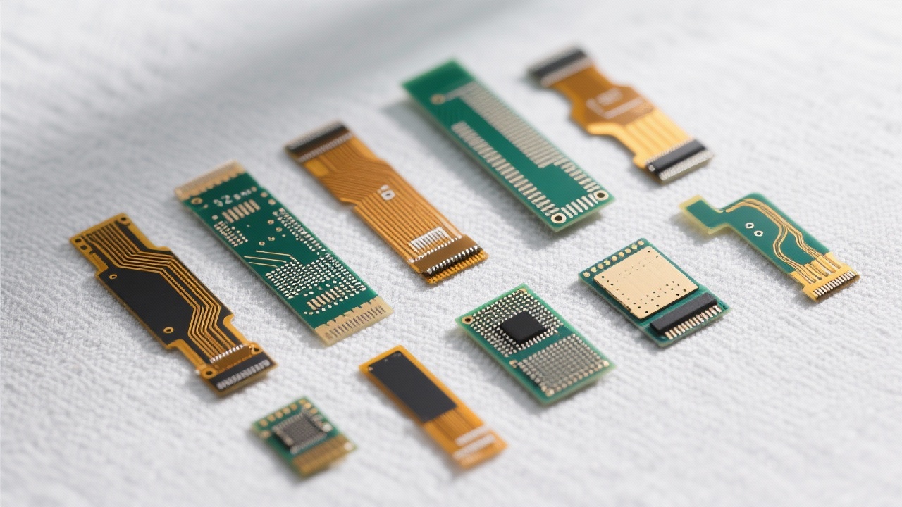
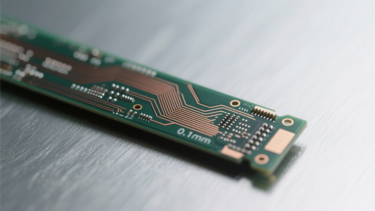
Flexible circuits must balance extreme miniaturization with mechanical resilience, especially in single-sided, double-sided, and multi-layer configurations. A fundamental bottleneck lies in trace spacing and via sizing. Industry-leading standards push line widths and spaces down to 100 microns (0.1 mm), requiring meticulous control over fabrication tolerances. Overly aggressive routing without process accommodation can lead to signal degradation or manufacturing defects.
In addition, the design of vias and microvias—those tiny plated-through holes connecting layers—is critical. Utilizing through-holes as small as 0.2 mm diameters demands precise drilling and plating processes combined with thorough inspection protocols to avoid voids or fractures. Adequate annular ring dimensions and aspect ratios must be respected to ensure robust electrical and mechanical connections.
High-density routing inherently increases the risk of signal crosstalk and electromagnetic interference (EMI). Applying design rules such as controlled impedance traces, separation of analog and digital signals, and careful ground plane arrangements are essential. Industry experts advise maintaining differential pair symmetry and incorporating ground shielding traces to effectively reduce noise coupling.
Robust electromagnetic compatibility (EMC) arises from both circuit design and material selection. Deploying lightweight, low-dielectric-constant substrates improves high-frequency signal transmission while minimizing parasitic capacitance. Layer stacking sequences further contribute to EMI containment by optimizing return current paths.
Modern FPC fabrication leverages advanced laser and mechanical micro-drilling equipment capable of producing consistent holes as small as 0.2 mm with tight tolerances. The plating process for microvias requires meticulous control to prevent incomplete fill or delamination issues.
Material innovations also support these demands. The use of ultra-thin polyimide substrates, combined with tailored copper foil thicknesses, reduces flexural stress without sacrificing electrical performance. Special adhesive layers with enhanced thermal and mechanical properties help maintain integrity through repeated bending cycles.
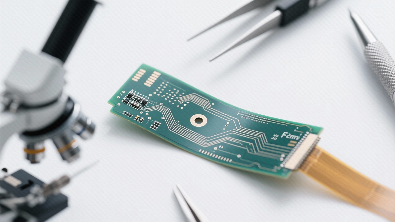
One critical reliability factor is stress management in flex zones. Engineering design integration of bend radius specifications and reinforcement strategies, alongside accelerated lifecycle testing protocols, ensure consistent long-term durability.
Backed by a dedicated team of 55 research and development engineers and an ISO-certified quality management system, our organization has delivered over 400 high-density FPC solutions to global clients. This wealth of experience translates into proven methodologies covering design optimization, manufacturing feasibility, and rigorous electrical and mechanical validation.
Industry standards continue to evolve, but foundational best practices — precise line and via dimensioning, signal isolation, material selection, and reliability testing — remain paramount for successful development and volume production of advanced FPCs.
 402
|
402
|
 FPC high-density routing
flexible circuit board design tips
EMC optimization
high-density PCB trace spacing
flexible printed circuit manufacturing
459
|
Multilayer FPC Via Design
FPC Bend Area Stress
Flexible Circuit Design
High-Density FPC Routing
FPC Reliability Enhancement
412
|
double layer PCB rapid manufacturing
PCB surface finishing technologies
flying probe testing
PCB production process
electrical reliability testing
256
|
multilayer flexible pcb via design
high-density fpc routing
fpc electromagnetic compatibility
flexible circuit board manufacturing capability
fpc bend zone reliability
325
|
FPC high - density wiring
Flexible circuit board design skills
Via design challenges
Electromagnetic compatibility optimization
Flexible PCB manufacturing process
FPC high-density routing
flexible circuit board design tips
EMC optimization
high-density PCB trace spacing
flexible printed circuit manufacturing
459
|
Multilayer FPC Via Design
FPC Bend Area Stress
Flexible Circuit Design
High-Density FPC Routing
FPC Reliability Enhancement
412
|
double layer PCB rapid manufacturing
PCB surface finishing technologies
flying probe testing
PCB production process
electrical reliability testing
256
|
multilayer flexible pcb via design
high-density fpc routing
fpc electromagnetic compatibility
flexible circuit board manufacturing capability
fpc bend zone reliability
325
|
FPC high - density wiring
Flexible circuit board design skills
Via design challenges
Electromagnetic compatibility optimization
Flexible PCB manufacturing process
-4.png?x-oss-process=image/resize,h_800,m_lfit/format,webp)

-1.png?x-oss-process=image/resize,h_800,m_lfit/format,webp)


-1.png?x-oss-process=image/resize,m_fill,h_800,w_800/format,webp)
-L4-4.png?x-oss-process=image/resize,m_fill,h_800,w_800/format,webp)


-4.png?x-oss-process=image/resize,m_fill,h_800,w_800/format,webp)