
In the era of rapid development of 5G and high - frequency communication, the impedance stability of high - speed multi - layer PCBs directly determines signal integrity and system reliability. This article aims to provide in - depth insights into the key factors affecting impedance stability in high - speed PCBs, which is crucial for engineers in the telecommunications industry.
Impedance control is the process of ensuring that the electrical impedance of a PCB trace matches the source and load impedance. In high - speed signal transmission, any impedance mismatch can lead to signal reflections, which degrade signal quality and may cause system malfunctions. For example, in a 5G base station PCB, where high - speed data transfer is essential, maintaining proper impedance is like building a smooth highway for data flow.
The 50 - ohm single - ended impedance is widely used in single - ended signal transmission lines, such as power supply lines and some low - frequency single - ended signal lines. On the other hand, the 100 - ohm differential impedance is commonly used in high - speed differential signal pairs, like USB 3.0 and Ethernet interfaces. The design of these impedance values is based on a balance between signal integrity, power consumption, and the characteristics of the transmission medium.
Key Conclusion: The selection of 50 - ohm single - ended and 100 - ohm differential impedance is determined by the specific application requirements and the nature of the high - speed signals.
Material properties, such as dielectric constant and loss factor, play a significant role in impedance stability. High - performance dielectric materials like ISOLA 370HR and MENTRON6 have stable dielectric constants, which help maintain consistent impedance values across the PCB. A lower loss factor means less signal attenuation during transmission, further enhancing signal integrity. For instance, a change in the dielectric constant of just 0.1 can cause a significant shift in impedance, which may lead to signal quality issues.
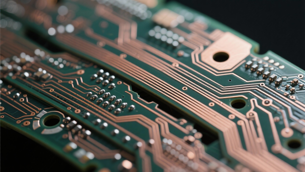
Manufacturing tolerances, including line width/spacing, copper thickness, and via filling, are critical for impedance control. For example, a 3mil line width/spacing and 20mil BGA pads require high - precision manufacturing processes. Even a small deviation in line width can cause impedance variations. Copper thickness also affects impedance, as a thicker copper layer may reduce resistance but can also change the impedance characteristics. Via filling is essential to ensure proper electrical connection and impedance continuity.
Key Conclusion: Precise manufacturing processes are necessary to meet the strict impedance requirements of high - speed PCBs.
Advanced measurement means, such as design simulation and AOI (Automated Optical Inspection) testing, are essential for ensuring impedance consistency and improving yield. Design simulation can predict impedance values before manufacturing, allowing engineers to optimize the PCB design. AOI testing can detect any manufacturing defects that may affect impedance, such as short circuits or open circuits. By using these methods, the yield of high - quality PCBs can be increased from around 70% to over 90%.
The 24 - layer high - frequency PCB offered by our company has gained a strong reputation in the telecommunications industry for its reliability. Our PCBs are designed and manufactured with the highest precision, ensuring stable impedance and excellent signal integrity. If you are looking for high - quality PCBs for your next high - frequency application, we are here to help.
Click here to learn how we achieve stable impedance with precision manufacturing
 220
|
220
|
 FPC Hochdichte-Wirng
Flex-PCB-Design-Tipps
EMC-Optimierung
Hochdichte-Leitungsrouting-Lösungen
Flex-PCB-Fertigungstechnologie
360
|
FPC Hochdichte Leiterbahnen
Flexible Leiterplatten Design
Elektromagnetische Verträglichkeit FPC
Hochpräzise FPC Fertigung
FPC Zuverlässigkeit
96
|
FPC Hochdichte - Verdrahtung
Flexibles Leiterplatten - Entwurfstechniken
Optimierung der elektromagnetischen Verträglichkeit
Hochdichte - flexible Leiterplatten
Fertigungsprozesse für mehrlagige FPC
447
|
Hochdichte Verdrahtung von FPC
Entwurfstechniken für flexible Leiterplatten
Optimierung der elektromagnetischen Verträglichkeit
Hochdichte flexible PCB
Via - Entwurfstandards
229
|
Impedanzkontrolle
Hochgeschwindigkeits-PCB-Design
5G-Basisstation-PCB
Signalintegrität
Hochfrequenz-PCB-Herstellung
FPC Hochdichte-Wirng
Flex-PCB-Design-Tipps
EMC-Optimierung
Hochdichte-Leitungsrouting-Lösungen
Flex-PCB-Fertigungstechnologie
360
|
FPC Hochdichte Leiterbahnen
Flexible Leiterplatten Design
Elektromagnetische Verträglichkeit FPC
Hochpräzise FPC Fertigung
FPC Zuverlässigkeit
96
|
FPC Hochdichte - Verdrahtung
Flexibles Leiterplatten - Entwurfstechniken
Optimierung der elektromagnetischen Verträglichkeit
Hochdichte - flexible Leiterplatten
Fertigungsprozesse für mehrlagige FPC
447
|
Hochdichte Verdrahtung von FPC
Entwurfstechniken für flexible Leiterplatten
Optimierung der elektromagnetischen Verträglichkeit
Hochdichte flexible PCB
Via - Entwurfstandards
229
|
Impedanzkontrolle
Hochgeschwindigkeits-PCB-Design
5G-Basisstation-PCB
Signalintegrität
Hochfrequenz-PCB-Herstellung


-L4-4.png?x-oss-process=image/resize,m_fill,h_800,w_800/format,webp)


-4.png?x-oss-process=image/resize,h_800,m_lfit/format,webp)


