
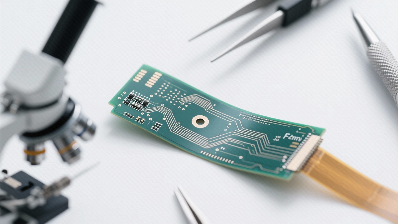
In high - density application scenarios such as consumer electronics and medical devices, optimizing the electromagnetic compatibility (EMC) and protecting against signal crosstalk of flexible printed circuit boards (FPCs) have become crucial for the success of the design. This article delves into real - world customer cases to illustrate how to enhance signal integrity through layout optimization, trace spacing control (minimum of 0.1mm), via design, and shielding structures. Meanwhile, by integrating precision manufacturing processes (e.g., minimum via diameter of 0.2mm), we can achieve high - reliability mass production, enabling engineers to comprehensively master the core logic and practical skills of high - density FPC wiring from theory to engineering practice.
When dealing with high - density FPC wiring, engineers often encounter three major technical challenges: avoiding layout interference, controlling trace spacing, and managing via stress. Layout interference can significantly affect the performance of the entire circuit, as improper component placement can lead to signal interference and reduced efficiency. Trace spacing control is also vital, as insufficient spacing can cause signal crosstalk, which may result in data errors and system malfunctions. Via stress management is another critical aspect, as excessive stress on vias can lead to cracks and other reliability issues.
Let's take a real customer project as an example. In this case, the customer had an FPC design that suffered from severe EMC problems, which led to unstable system operation. Our team first identified the root causes of the EMC issues through a systematic process. We found that the improper ground plane segmentation, non - optimal differential pair routing, and lack of an effective shielding layer were the main culprits.
Customer Case: A leading consumer electronics company approached us with an FPC design for a new smartphone. The device was experiencing intermittent signal loss and electromagnetic interference, which affected its overall performance. Our experts analyzed the design and implemented solutions such as proper ground plane segmentation, optimized differential pair routing, and the addition of a shielding layer. After the improvements, the EMC performance of the FPC was significantly enhanced, and the smartphone passed all the required electromagnetic compatibility tests.
To solve these problems, we adopted practical strategies such as proper ground plane segmentation, which helps to reduce electromagnetic interference. Differential pair routing was optimized to ensure balanced signal transmission, and a well - designed shielding layer was added to protect the signals from external interference. These measures effectively improved the EMC performance of the FPC.
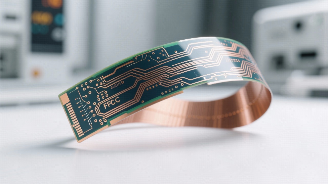
Manufacturing capabilities play a crucial role in realizing complex FPC designs. For example, a minimum via diameter of 0.2mm and a line width/spacing of 0.1mm/0.1mm are essential for ensuring signal integrity. These high - precision manufacturing processes can effectively reduce signal attenuation and crosstalk, thereby improving the overall performance and reliability of the FPC.
Our advanced manufacturing facilities are capable of achieving these high - precision requirements, ensuring that even the most complex FPC designs can be mass - produced with high quality and consistency. We have already successfully implemented such solutions for many leading customers, providing them with reliable FPC products that meet their strict performance requirements.
There are significant differences in stress distribution between traditional rigid PCBs and flexible PCBs in bent areas. To enhance the reliability of flexible PCBs, we propose specific solutions such as R - corner processing and material selection. R - corner processing can effectively reduce stress concentration in bent areas, while proper material selection can improve the flexibility and durability of the FPC.
We emphasize the advantages of one - stop R & D + manufacturing collaboration, which can help customers efficiently complete the entire process from prototype verification to mass delivery. Our integrated approach allows for seamless communication between the R & D and manufacturing teams, ensuring that design requirements are accurately translated into high - quality products.
Our R & D team can provide customized EMC optimization suggestions based on the specific needs of each customer. We have extensive experience in dealing with various FPC design challenges and can offer practical solutions to help our customers achieve their goals.
 53
|
53
|
 high-density FPC routing
flexible PCB design techniques
EMI optimization in FPC
precision via design for flexible circuits
FPC manufacturing process
247
|
FPC high-density routing
flexible circuit board design
trace spacing control
EMI shielding in FPC
flexible PCB manufacturing
159
|
high-density FPC design
flexible PCB signal integrity
EMI optimization in FPC
signal crosstalk prevention
microvia fabrication in flexible PCB
360
|
High-density FPC routing
Flexible circuit board design
Electromagnetic compatibility optimization
Precision FPC manufacturing
Flexible PCB reliability
339
|
FPC high-density wiring
Flexible circuit board design skills
Electromagnetic compatibility optimization
Flexible PCB manufacturing process
High-density printed circuit board
high-density FPC routing
flexible PCB design techniques
EMI optimization in FPC
precision via design for flexible circuits
FPC manufacturing process
247
|
FPC high-density routing
flexible circuit board design
trace spacing control
EMI shielding in FPC
flexible PCB manufacturing
159
|
high-density FPC design
flexible PCB signal integrity
EMI optimization in FPC
signal crosstalk prevention
microvia fabrication in flexible PCB
360
|
High-density FPC routing
Flexible circuit board design
Electromagnetic compatibility optimization
Precision FPC manufacturing
Flexible PCB reliability
339
|
FPC high-density wiring
Flexible circuit board design skills
Electromagnetic compatibility optimization
Flexible PCB manufacturing process
High-density printed circuit board
-4.png?x-oss-process=image/resize,h_800,m_lfit/format,webp)
-1.png?x-oss-process=image/resize,h_800,m_lfit/format,webp)


-4.png?x-oss-process=image/resize,m_fill,h_800,w_800/format,webp)


-L4-4.png?x-oss-process=image/resize,m_fill,h_800,w_800/format,webp)