Dual-Layer PCB Rapid Manufacturing Process: From Design to Flying Probe Testing Explained

Ruiheng PCB
2026-02-04
Technical knowledge
How can dual-layer PCB rapid manufacturing achieve both efficiency and high quality? This article provides a comprehensive breakdown of the full production workflow—from design input to flying probe testing—with technical insights on etching precision, layer press consistency, drilling tolerance management, and surface treatment differences between LF HAL, ENIG, and OSP. It also highlights the role of flying probe testing in electrical reliability validation and explains how in-house production and global logistics enable faster delivery and better control for electronics manufacturers.
https://shmuker.oss-accelerate.aliyuncs.com/data/oss/20251230/e27c0d48147daaf89d42615115b5f11b/45f97e58-2cdb-4b1e-8901-1445a87ab7e5.jpeg

The Key to Fast & Reliable Double-Layer PCB Manufacturing: A Process Deep Dive

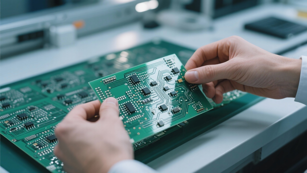
For electronics engineers and procurement managers seeking rapid prototyping without compromising quality, double-layer PCBs remain a cornerstone of modern product development. But how do leading manufacturers balance speed with precision? This article breaks down the end-to-end process—from design input to fly probe testing—with actionable insights on optimizing each stage for faster turnaround and higher reliability.

Step-by-Step Breakdown: From Design to Final Test

The journey begins with Gerber file validation—a step often overlooked but critical for avoiding costly rework. Once validated, the copper etching phase must maintain ±5μm tolerance across all traces to ensure signal integrity in high-frequency applications. At this point, layer alignment during lamination becomes crucial: poor consistency can lead to delamination under thermal stress, especially in automotive or industrial-grade boards.

Drilling accuracy follows closely—typically ±0.05mm for standard through-hole components, though precision connectors may demand tighter tolerances (±0.02mm). Our internal data shows that using automated drilling machines reduces setup time by up to 40% compared to manual methods, directly impacting overall cycle time from 7 days to just 4 days for small batches.

Flowchart showing key stages in double-layer PCB manufacturing: Design Input → Etching → Lamination → Drilling → Surface Treatment → Fly Probe Testing

Surface Finishes Matter: Choosing the Right One

Three surface treatments dominate the market:

  • LF HAL (Lead-Free Hot Air Leveling): Ideal for general-purpose boards with cost-sensitive buyers—offers good solderability and is widely supported globally.
  • ENIG (Electroless Nickel Immersion Gold): Preferred for fine-pitch BGA and HDI designs due to superior planarity and shelf life (up to 12 months).
  • OSP (Organic Solderability Preservative): Eco-friendly option for low-volume prototypes; however, it requires careful storage and has shorter shelf life (~6 months).

We’ve seen clients switch from HAL to ENIG when moving from prototype to volume production—they report fewer solder joint failures and improved test yield rates by 15–20%.

Why In-House Production Wins

Manufacturers who control their entire production chain—from raw material sourcing to final inspection—can reduce lead times by 30–50%. Unlike outsourced models where bottlenecks occur at multiple handoffs, vertical integration ensures consistent QC checks at every stage. For example, our facility uses real-time AOI (Automated Optical Inspection) after plating, catching defects before they reach the fly probe station.

In one case study, a medical device client reduced PCB delivery time from 14 days to 5 days by leveraging our integrated workflow and global logistics network—without sacrificing compliance with IPC-6012 standards.

Comparison chart showing average delivery times for PCBs made in-house vs. outsourced facilities

Ultimately, the ability to iterate quickly while maintaining electrical performance hinges not just on technology—but on process discipline. Whether you're designing a new IoT sensor or scaling up an existing product line, understanding these technical nuances empowers smarter decisions.

“We base our recommendations on years of hands-on experience—not theory. If your project needs fast, reliable double-layer PCBs, we can tailor the process to your specific requirements.”

Ready to Accelerate Your PCB Development?

Get expert guidance tailored to your project’s unique needs—no pressure, just clarity.

Explore Our Custom PCB Solutions
Name *
Email *
Message*

Recommended Products

Related Reading

Mastering High-Density Routing in FPC Design: Techniques for Optimized Layout and Signal Integrity

2026-01-10 | https://shmuker.oss-accelerate.aliyuncs.com/tmp/temporary/60ec5bd7f8d5a86c84ef79f2/60ec5bdcf8d5a86c84ef7a9a/20240305161110/eye.png 53 | https://shmuker.oss-accelerate.aliyuncs.com/tmp/temporary/60ec5bd7f8d5a86c84ef79f2/60ec5bdcf8d5a86c84ef7a9a/20240305160636/lable.png high-density FPC routing flexible PCB design techniques EMI optimization in FPC precision via design for flexible circuits FPC manufacturing process

High-Speed Multilayer PCB Impedance Measurement and AOI Detection Technology Tutorial: Enhance Product Quality and Signal Integrity

2026-01-28 | https://shmuker.oss-accelerate.aliyuncs.com/tmp/temporary/60ec5bd7f8d5a86c84ef79f2/60ec5bdcf8d5a86c84ef7a9a/20240305161110/eye.png 315 | https://shmuker.oss-accelerate.aliyuncs.com/tmp/temporary/60ec5bd7f8d5a86c84ef79f2/60ec5bdcf8d5a86c84ef7a9a/20240305160636/lable.png High-speed multilayer PCB Impedance control technology AOI detection Signal integrity 5G communication PCB

Master Multilayer Flexible PCB Via Design for High-Density Routing in Consumer Electronics and Medical Devices

2025-12-30 | https://shmuker.oss-accelerate.aliyuncs.com/tmp/temporary/60ec5bd7f8d5a86c84ef79f2/60ec5bdcf8d5a86c84ef7a9a/20240305161110/eye.png 256 | https://shmuker.oss-accelerate.aliyuncs.com/tmp/temporary/60ec5bd7f8d5a86c84ef79f2/60ec5bdcf8d5a86c84ef7a9a/20240305160636/lable.png multilayer flexible pcb via design high-density fpc routing fpc electromagnetic compatibility flexible circuit board manufacturing capability fpc bend zone reliability

Research on Via Design Challenges and Manufacturing Process Support in High-Density Wiring of Multi-Layer Flexible Circuit Boards

2026-01-02 | https://shmuker.oss-accelerate.aliyuncs.com/tmp/temporary/60ec5bd7f8d5a86c84ef79f2/60ec5bdcf8d5a86c84ef7a9a/20240305161110/eye.png 325 | https://shmuker.oss-accelerate.aliyuncs.com/tmp/temporary/60ec5bd7f8d5a86c84ef79f2/60ec5bdcf8d5a86c84ef7a9a/20240305160636/lable.png FPC high - density wiring Flexible circuit board design skills Via design challenges Electromagnetic compatibility optimization Flexible PCB manufacturing process

Advanced Via Design and Micro-Hole Processing in Multilayer Flexible PCBs: A Comprehensive Guide

2026-01-07 | https://shmuker.oss-accelerate.aliyuncs.com/tmp/temporary/60ec5bd7f8d5a86c84ef79f2/60ec5bdcf8d5a86c84ef7a9a/20240305161110/eye.png 156 | https://shmuker.oss-accelerate.aliyuncs.com/tmp/temporary/60ec5bd7f8d5a86c84ef79f2/60ec5bdcf8d5a86c84ef7a9a/20240305160636/lable.png multilayer flexible pcb via design micro-hole processing in fpc high-density flex pcb layout emc optimization in flexible circuits flexible pcb manufacturing process
Popular articles
https://shmuker.oss-accelerate.aliyuncs.com/data/oss/692910f1af15994642dab58b/692a498eaf15994642dace1b/20251216172341/FR4-PI-Steel-Reinforced-Flexible-Circuit-Board-(FPC)-1.png
https://shmuker.oss-accelerate.aliyuncs.com/data/oss/20251230/108753c856212ca24423e047f1fae39d/aaca0d0a-903c-4a00-8d92-9c30893b54c5.jpeg
https://shmuker.oss-accelerate.aliyuncs.com/data/oss/20251230/74cae3ecdb9a0b7f18e44f6631cea9fa/a50611de-8ff5-4f46-a7e1-6a2a52b90b99.jpeg
https://shmuker.oss-accelerate.aliyuncs.com/data/oss/20251230/141e3615b7cc68db7aeef60572ce0a5a/df049d1d-21f7-4162-8696-74640563c4d1.jpeg
https://shmuker.oss-accelerate.aliyuncs.com/data/oss/692910f1af15994642dab58b/692a498eaf15994642dace1b/20251216152709/24-layer-circuit-board-4.png
https://shmuker.oss-accelerate.aliyuncs.com/data/oss/20251230/5c69fdd5ace28e3cea2fb4c117e4557a/b1df2e5c-4f37-4544-a170-ad2d4e887ce0.jpeg
https://shmuker.oss-accelerate.aliyuncs.com/data/oss/20251230/8b8b1d37b71e344d6a5f246185ce2506/34fa0194-4837-4f46-a9a0-4f56a966047d.jpeg
https://shmuker.oss-accelerate.aliyuncs.com/data/oss/20251230/f546ee23d1f5b79cb30ea144c64bf7a0/41080766-f5fe-4275-980d-2f6b2674b30f.jpeg
https://shmuker.oss-accelerate.aliyuncs.com/data/oss/20251230/10162eed1c55dc9d2c2f47a0acfd4f76/514a91c4-e6c4-488d-a6e8-0a112d4b66b7.jpeg
https://shmuker.oss-accelerate.aliyuncs.com/data/oss/20251230/76402db4ddda640df1d8ea772a31c807/0ec0487d-c513-4ae1-bddb-49f7de806bce.jpeg
Recommended Reading
Contact us
Contact us
https://shmuker.oss-accelerate.aliyuncs.com/tmp/temporary/60ec5bd7f8d5a86c84ef79f2/60ec5bdcf8d5a86c84ef7a9a/thumb-prev.png