ENIG Surface Finish Technology Explained: Enhancing Solder Reliability in High-Density Flexible PCBs

Ruiheng PCB
2026-03-16
Technical knowledge
This article provides a comprehensive overview of Electroless Nickel Immersion Gold (ENIG) surface finish technology in high-density flexible printed circuit boards (FPCs). It details the process flow, material selection, and critical parameters such as nickel and gold layer thickness, purity, and surface roughness—highlighting how these factors directly impact solder joint reliability, corrosion resistance, and signal integrity. By comparing ENIG with OSP, HASL, and ENEPIG, this guide clarifies each method’s advantages and ideal applications. Real-world cases from smartphone motherboards and aerospace electronics demonstrate ENIG’s role in precise impedance control and performance stability under extreme conditions. Industry standards like RoHS, UL, and IATF 16949 are also reviewed to ensure compliance and reduce risk. With technical diagrams and microstructure images, this piece supports engineers and procurement professionals in making informed decisions for advanced FPC solutions—backed by Ruiheng PCB’s commitment to quality and innovation.
https://shmuker.oss-accelerate.aliyuncs.com/data/oss/20251230/6361a7640bda96ec7b6928195a7b0ab9/0cff8b23-5c1d-4865-9c37-40619b2a114b.jpeg

ENIG Surface Finish: The Secret to Reliable High-Density Flexible PCBs

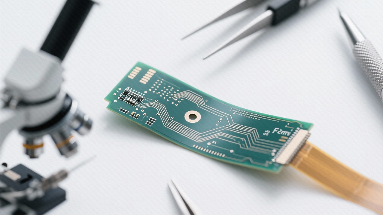
In today’s high-speed electronics—from smartphones to aerospace systems—flexible printed circuit boards (FPCs) are no longer optional. They’re essential. But how do you ensure consistent solder joint reliability and signal integrity when your circuits push the limits of miniaturization? The answer lies in one critical process: Electroless Nickel Immersion Gold (ENIG).

Why ENIG Matters for Modern FPC Design

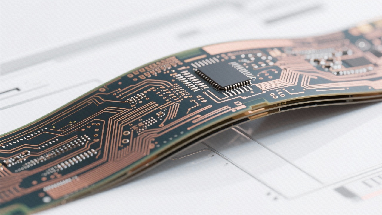
ENIG isn’t just another surface treatment—it’s a precision-engineered solution that addresses two core challenges in high-density flexible PCB manufacturing: solderability and corrosion resistance. With nickel layers typically between 3–5 μm thick and gold coatings around 0.05–0.1 μm, ENIG delivers a flat, uniform finish ideal for micro-via interconnects and fine-pitch components.

Studies show that properly executed ENIG can reduce solder joint failure rates by up to 40% compared to OSP or HASL in repeated thermal cycling tests—a key metric for devices expected to last years under stress.

Cross-section diagram showing ENIG layer structure on flexible PCB substrate: copper → nickel plating → thin gold layer.

How ENIG Outperforms Other Surface Finishes

Surface Finish Solder Reliability Cost Efficiency Best Use Case
ENIG High (ideal for fine pitch) Moderate Smartphones, medical devices
OSP Low-Medium (short shelf life) Low Consumer-grade PCBs
HASL Medium (uneven surface) Low Industrial controls

For applications requiring tight impedance control—like 5G modules or satellite communication systems—ENIG offers superior consistency over time. Its low surface roughness (<0.5 μm Ra) minimizes signal loss, making it a preferred choice among top-tier manufacturers like Ruiheng PCB.

Microscopic view of ENIG-treated solder joints showing smooth, uniform morphology without voids or cracks.

Compliance That Builds Trust

Global compliance standards such as RoHS, UL, and IATF 16949 aren’t just checkboxes—they’re trust signals. ENIG processes must meet strict thresholds for lead content (<100 ppm), halogen-free materials, and dimensional stability across temperature cycles (-40°C to +125°C). These specs are non-negotiable in automotive and aerospace sectors where failure means cost—and risk.

Ruiheng PCB has successfully implemented ENIG across multiple production lines with consistent yield rates above 97%, thanks to real-time monitoring of bath chemistry, pH, and temperature during plating. This level of process control ensures not only product quality but also long-term supply chain resilience.

Ready to Deepen Your Understanding?

Download our comprehensive technical white paper on ENIG surface finishes in flexible PCBs—including detailed case studies from smartphone OEMs and aerospace suppliers.

Get the Full Technical Guide Now
Name *
Email *
Message*

Recommended Products

Related Reading

Professional High-Speed Multilayer PCB Manufacturing Solutions for Efficient Impedance Control and Signal Optimization in 5G Communication Devices

2026-01-29 | https://shmuker.oss-accelerate.aliyuncs.com/tmp/temporary/60ec5bd7f8d5a86c84ef79f2/60ec5bdcf8d5a86c84ef7a9a/20240305161110/eye.png 350 | https://shmuker.oss-accelerate.aliyuncs.com/tmp/temporary/60ec5bd7f8d5a86c84ef79f2/60ec5bdcf8d5a86c84ef7a9a/20240305160636/lable.png High - speed multilayer PCB Impedance control 5G communication PCB Signal integrity High - frequency PCB manufacturing

How 0.3mm PI Reinforcement Edge Design Reduces Stress Concentration in Industrial FPC Bending Failures

2026-03-10 | https://shmuker.oss-accelerate.aliyuncs.com/tmp/temporary/60ec5bd7f8d5a86c84ef79f2/60ec5bdcf8d5a86c84ef7a9a/20240305161110/eye.png 206 | https://shmuker.oss-accelerate.aliyuncs.com/tmp/temporary/60ec5bd7f8d5a86c84ef79f2/60ec5bdcf8d5a86c84ef7a9a/20240305160636/lable.png FPC bending failure analysis PI reinforcement edge design stress concentration in flexible circuits SMT reflow soldering for FPC industrial FPC reliability

Optimizing Four-Layer Thick Copper PCB Design for Enhanced Power Electronics Thermal Management

2026-02-20 | https://shmuker.oss-accelerate.aliyuncs.com/tmp/temporary/60ec5bd7f8d5a86c84ef79f2/60ec5bdcf8d5a86c84ef7a9a/20240305161110/eye.png 402 | https://shmuker.oss-accelerate.aliyuncs.com/tmp/temporary/60ec5bd7f8d5a86c84ef79f2/60ec5bdcf8d5a86c84ef7a9a/20240305160636/lable.png four-layer thick copper PCB design power electronics PCB thermal optimization thick copper PCB minimum trace spacing ENIG surface finish benefits high Tg FR-4 applications

0.1mm Microvias & 0.5mm Backdrilling: Synergistic Control in High-End HDI PCB Manufacturing

2026-02-14 | https://shmuker.oss-accelerate.aliyuncs.com/tmp/temporary/60ec5bd7f8d5a86c84ef79f2/60ec5bdcf8d5a86c84ef7a9a/20240305161110/eye.png 479 | https://shmuker.oss-accelerate.aliyuncs.com/tmp/temporary/60ec5bd7f8d5a86c84ef79f2/60ec5bdcf8d5a86c84ef7a9a/20240305160636/lable.png HDI PCB Manufacturing 0.1mm Microvia Process 0.5mm Backdrilling Technology PCB Microvia Formation IPC-III Standard

High-Precision 4-Layer FPC Design: Achieving 2mil Trace Width and Spacing

2026-03-15 | https://shmuker.oss-accelerate.aliyuncs.com/tmp/temporary/60ec5bd7f8d5a86c84ef79f2/60ec5bdcf8d5a86c84ef7a9a/20240305161110/eye.png 227 | https://shmuker.oss-accelerate.aliyuncs.com/tmp/temporary/60ec5bd7f8d5a86c84ef79f2/60ec5bdcf8d5a86c84ef7a9a/20240305160636/lable.png high-precision FPC design 2mil trace width 4-layer flexible PCB ENIG surface finish impedance control
Popular articles
https://shmuker.oss-accelerate.aliyuncs.com/data/oss/20251230/141e3615b7cc68db7aeef60572ce0a5a/df049d1d-21f7-4162-8696-74640563c4d1.jpeg
https://shmuker.oss-accelerate.aliyuncs.com/data/oss/20251230/108753c856212ca24423e047f1fae39d/aaca0d0a-903c-4a00-8d92-9c30893b54c5.jpeg
https://shmuker.oss-accelerate.aliyuncs.com/data/oss/20251230/6361a7640bda96ec7b6928195a7b0ab9/0cff8b23-5c1d-4865-9c37-40619b2a114b.jpeg
https://shmuker.oss-accelerate.aliyuncs.com/data/oss/20251230/f546ee23d1f5b79cb30ea144c64bf7a0/41080766-f5fe-4275-980d-2f6b2674b30f.jpeg
https://shmuker.oss-accelerate.aliyuncs.com/data/oss/20251230/5c69fdd5ace28e3cea2fb4c117e4557a/b1df2e5c-4f37-4544-a170-ad2d4e887ce0.jpeg
https://shmuker.oss-accelerate.aliyuncs.com/data/oss/20251230/108753c856212ca24423e047f1fae39d/aaca0d0a-903c-4a00-8d92-9c30893b54c5.jpeg
https://shmuker.oss-accelerate.aliyuncs.com/data/oss/20251230/10162eed1c55dc9d2c2f47a0acfd4f76/514a91c4-e6c4-488d-a6e8-0a112d4b66b7.jpeg
https://shmuker.oss-accelerate.aliyuncs.com/data/oss/20251230/f546ee23d1f5b79cb30ea144c64bf7a0/41080766-f5fe-4275-980d-2f6b2674b30f.jpeg
https://shmuker.oss-accelerate.aliyuncs.com/data/oss/20251230/5c69fdd5ace28e3cea2fb4c117e4557a/b1df2e5c-4f37-4544-a170-ad2d4e887ce0.jpeg
https://shmuker.oss-accelerate.aliyuncs.com/data/oss/20251230/6361a7640bda96ec7b6928195a7b0ab9/0cff8b23-5c1d-4865-9c37-40619b2a114b.jpeg
Recommended Reading
Contact us
Contact us
https://shmuker.oss-accelerate.aliyuncs.com/tmp/temporary/60ec5bd7f8d5a86c84ef79f2/60ec5bdcf8d5a86c84ef7a9a/thumb-prev.png