Comprehensive Guide to Fast Double-Sided PCB Manufacturing: From Design to Final Testing

Ruiheng PCB
2026-02-05
Tutorial Guide
This article provides an in-depth analysis of the fast manufacturing process and essential technical aspects of double-sided PCBs. Covering critical stages from design input, etching, lamination, drilling, to surface finishing and flying probe testing, it offers detailed insights into key surface treatment methods including LF HAL, ENIG, and OSP. Emphasizing the benefits of in-house production capabilities, the guide highlights quality control improvements and shortened delivery cycles. Supported by diagrams and real-world examples, it serves as a vital resource for electronics engineers and production managers aiming to optimize PCB manufacturing and supply chain efficiency for rapid global market response.
https://shmuker.oss-accelerate.aliyuncs.com/data/oss/20251230/74cae3ecdb9a0b7f18e44f6631cea9fa/a50611de-8ff5-4f46-a7e1-6a2a52b90b99.jpeg

Comprehensive Guide to Rapid Manufacturing of Double-Sided PCBs: From Design Input to Final Testing

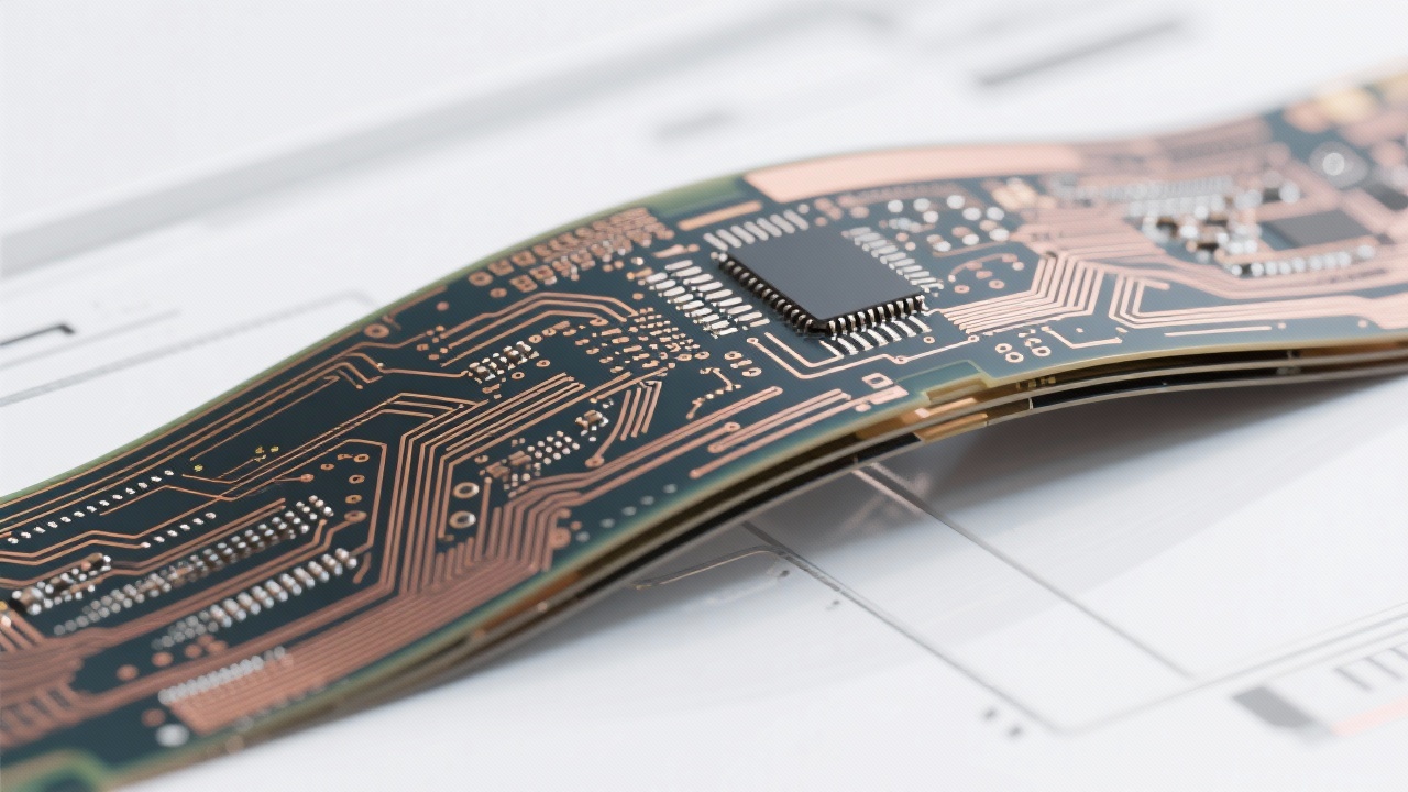
In today’s fast-paced electronics industry, the demand for high-quality, double-sided printed circuit boards (PCBs) with rapid turnaround times continues to surge. This guide explores the critical technologies and process steps involved in efficiently manufacturing double-layer PCBs, emphasizing how precision at every stage—from design input to final electrical testing—ensures reliability and accelerates production cycles. Professionals in electronic engineering and production management will find this resource instrumental in optimizing their workflows and supply chain responsiveness.

1. Streamlining the Double-Layer PCB Manufacturing Workflow

Manufacturing double-layer PCBs involves several interdependent processes, each contributing to the overall quality and performance. The principal stages include:

  • Design Input: Clear and detailed Gerber files combined with precise drill data set the foundation for manufacturing accuracy.
  • Etching: Controlled chemical etching reproduces circuit patterns with micron-level precision; typical etch tolerance is ±0.05 mm.
  • Lamination: Layer bonding with high-temperature lamination machines ensures integrity and dielectric strength.
  • Drilling: CNC drilling with 0.15 mm minimum hole diameter capability supports high-density designs.
  • Surface Treatment: Application of protective finishes enhances solderability and prevents oxidation.
  • Testing: Flying probe (flying needle) testing verifies electrical continuity and identifies potential open or short circuits.

2. Etching, Lamination, and Drilling: Core Process Leadership

Etching stands as the most delicate step where precision defines the fidelity of circuit traces. Modern processes utilize automated spray etching and in-line inspection systems capable of real-time defect detection, boosting yield rates above 98%. In lamination, multi-layered prepregs are thermally compressed, forming robust dielectric bonds essential for board durability and electrical insulation.

High-speed CNC routers and laser drilling systems enable hole size control and positional accuracy within ±0.02 mm, adaptable to various PCB designs requiring vias and through-holes.

3. Surface Treatments: LF HAL, ENIG, and OSP Explained

Surface finishes protect copper pads and enhance solderability. Manufacturers must carefully select from three primary finishes based on application and cost considerations:

  1. Lead-Free Hot Air Leveling (LF HAL): Offers a reliable coating of solder on copper pads, suitable for wave soldering. Provides good mechanical strength but may have a shorter shelf life than other finishes.
  2. Electroless Nickel Immersion Gold (ENIG): Features a flat, corrosion-resistant surface ideal for fine-pitch components and surface mount technology (SMT). ENIG is favored in high-reliability applications due to excellent planarity and oxidation resistance.
  3. Organic Solderability Preservative (OSP): An economical, environmentally-friendly finish that protects the copper with a thin organic layer. Best applied in rapid manufacturing where just-in-time assembly reduces oxidation risk.
Technical diagram showing LF HAL, ENIG, and OSP surface treatments on double-layer PCBs

4. Flying Probe Testing: Ensuring Electrical Reliability Without Expensive Fixtures

Flying probe testing uses multiple needle probes that dynamically contact various pad points to detect opens, shorts, and critical faults. This non-contact method eliminates the need for costly bed-of-nails fixtures, reducing test setup times and enhancing flexibility for complex or small production batches.

Typical test durations range from 1 to 5 minutes per PCB depending on complexity, with defect detection rates exceeding 99%. The adaptive test program can be rapidly updated to match layout revisions, supporting agile production cycles.

Flying probe test equipment inspecting a double-layer PCB for electrical faults

5. Leveraging In-House Manufacturing for Quality Control and Faster Delivery

Owning the entire production chain—from material procurement to final testing—enables tighter quality control, reducing defect rates and rework by up to 25%. Internal manufacturing also shrinks lead times, with rapid prototyping and small-batch runs completed within 3-5 business days in many cases, drastically improving responsiveness to market demands.

Furthermore, synchronization of production schedules with optimized logistics leads to highly predictable order fulfillment, a critical competitive edge in global electronics supply chains.

6. Production Planning and Global Logistics: Case Insights

Optimized production workflows incorporate just-in-time (JIT) inventory management coupled with multi-modal global logistics tailored for time-sensitive electronics components. For example, integrating air freight with local last-mile delivery ensures orders reach customers within 7-10 days internationally, even during peak demand.

A recent case study revealed that adjusting batch sizes based on regional demand forecasts improved capacity utilization by 18%, while enhanced tracking systems reduced transit delays by nearly 30%. These data-driven adjustments have directly contributed to higher client satisfaction rates and repeat business.

Chart illustrating production timeline optimization and logistics efficiency for double-layer PCB delivery
Name *
Email *
Message*

Recommended Products

Related Reading

Enhance Flexible PCB Design Efficiency: High-Density Routing Solutions with Latest Manufacturing Processes

2026-01-14 | https://shmuker.oss-accelerate.aliyuncs.com/tmp/temporary/60ec5bd7f8d5a86c84ef79f2/60ec5bdcf8d5a86c84ef7a9a/20240305161110/eye.png 220 | https://shmuker.oss-accelerate.aliyuncs.com/tmp/temporary/60ec5bd7f8d5a86c84ef79f2/60ec5bdcf8d5a86c84ef7a9a/20240305160636/lable.png FPC high - density routing Flexible circuit board design techniques Electromagnetic compatibility optimization High - density routing solutions Flexible PCB manufacturing processes

Optimizing Electromagnetic Compatibility and Crosstalk Prevention in High-Density Flexible Printed Circuit Board Design

2026-01-06 | https://shmuker.oss-accelerate.aliyuncs.com/tmp/temporary/60ec5bd7f8d5a86c84ef79f2/60ec5bdcf8d5a86c84ef7a9a/20240305161110/eye.png 125 | https://shmuker.oss-accelerate.aliyuncs.com/tmp/temporary/60ec5bd7f8d5a86c84ef79f2/60ec5bdcf8d5a86c84ef7a9a/20240305160636/lable.png high-density FPC layout flexible PCB design techniques electromagnetic compatibility optimization signal crosstalk prevention advanced flexible PCB manufacturing

Multilayer FPC Via Design Essentials and Stress Concentration Mitigation in Bend Areas

2025-12-16 | https://shmuker.oss-accelerate.aliyuncs.com/tmp/temporary/60ec5bd7f8d5a86c84ef79f2/60ec5bdcf8d5a86c84ef7a9a/20240305161110/eye.png 459 | https://shmuker.oss-accelerate.aliyuncs.com/tmp/temporary/60ec5bd7f8d5a86c84ef79f2/60ec5bdcf8d5a86c84ef7a9a/20240305160636/lable.png Multilayer FPC Via Design FPC Bend Area Stress Flexible Circuit Design High-Density FPC Routing FPC Reliability Enhancement

From Design to Mass Production: Challenges and Solutions in High-Density Flexible PCB Manufacturing with a Minimum Hole Diameter of 0.2mm

2025-12-28 | https://shmuker.oss-accelerate.aliyuncs.com/tmp/temporary/60ec5bd7f8d5a86c84ef79f2/60ec5bdcf8d5a86c84ef7a9a/20240305161110/eye.png 41 | https://shmuker.oss-accelerate.aliyuncs.com/tmp/temporary/60ec5bd7f8d5a86c84ef79f2/60ec5bdcf8d5a86c84ef7a9a/20240305160636/lable.png FPC high-density wiring Flexible circuit board design techniques Electromagnetic compatibility optimization High-density flexible PCB manufacturing process Minimum hole diameter 0.2mm

Analysis of Practical Cases on Electromagnetic Compatibility Optimization and Signal Crosstalk Protection of Flexible PCBs

2026-01-11 | https://shmuker.oss-accelerate.aliyuncs.com/tmp/temporary/60ec5bd7f8d5a86c84ef79f2/60ec5bdcf8d5a86c84ef7a9a/20240305161110/eye.png 298 | https://shmuker.oss-accelerate.aliyuncs.com/tmp/temporary/60ec5bd7f8d5a86c84ef79f2/60ec5bdcf8d5a86c84ef7a9a/20240305160636/lable.png FPC high - density wiring Flexible circuit board design skills Electromagnetic compatibility optimization Signal crosstalk protection High - reliability FPC manufacturing
热门文章
https://shmuker.oss-accelerate.aliyuncs.com/data/oss/20251230/74cae3ecdb9a0b7f18e44f6631cea9fa/a50611de-8ff5-4f46-a7e1-6a2a52b90b99.jpeg
img
https://shmuker.oss-accelerate.aliyuncs.com/data/oss/20251230/141e3615b7cc68db7aeef60572ce0a5a/df049d1d-21f7-4162-8696-74640563c4d1.jpeg
https://shmuker.oss-accelerate.aliyuncs.com/data/oss/20251230/8b8b1d37b71e344d6a5f246185ce2506/34fa0194-4837-4f46-a9a0-4f56a966047d.jpeg
https://shmuker.oss-accelerate.aliyuncs.com/data/oss/20251230/76402db4ddda640df1d8ea772a31c807/0ec0487d-c513-4ae1-bddb-49f7de806bce.jpeg
https://shmuker.oss-accelerate.aliyuncs.com/data/oss/20251230/8b8b1d37b71e344d6a5f246185ce2506/34fa0194-4837-4f46-a9a0-4f56a966047d.jpeg
https://shmuker.oss-accelerate.aliyuncs.com/data/oss/20251230/72a89583d9313788c28e962d25e605bb/4168b1e5-33c6-487a-aab0-a253a7519936.jpeg
https://shmuker.oss-accelerate.aliyuncs.com/data/oss/20251230/76402db4ddda640df1d8ea772a31c807/0ec0487d-c513-4ae1-bddb-49f7de806bce.jpeg
https://shmuker.oss-accelerate.aliyuncs.com/data/oss/20251230/e27c0d48147daaf89d42615115b5f11b/45f97e58-2cdb-4b1e-8901-1445a87ab7e5.jpeg
img
Recommended Reading
Contact us
Contact us
https://shmuker.oss-accelerate.aliyuncs.com/tmp/temporary/60ec5bd7f8d5a86c84ef79f2/60ec5bdcf8d5a86c84ef7a9a/thumb-prev.png