
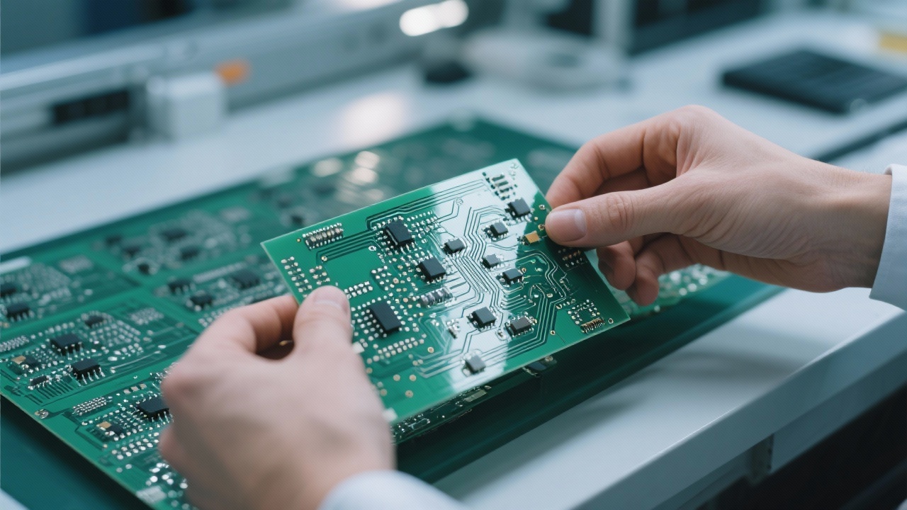
When designing high-reliability industrial electronics—such as medical imaging devices or automated control systems—the ability to consistently produce flexible printed circuits (FPCs) with a minimum line width and spacing of 0.05mm is no longer optional. It’s a technical benchmark that separates functional prototypes from mass-produced, field-ready products.
In modern industrial applications, signal integrity at frequencies above 1 GHz demands tight tolerances. A study by IPC-2221 shows that PCBs with line widths below 0.07mm experience up to 40% higher impedance variation under thermal stress—a critical issue for reliable data transmission. At 0.05mm, even minor deviations can cause crosstalk, signal loss, or premature failure in harsh environments like automotive or aerospace systems.
Key Process Parameter: For consistent 0.05mm lines, optical image transfer must achieve a resolution of ≥5 μm, while etching uniformity should be maintained within ±3% across the entire panel.
Our process combines advanced photolithography using UV-sensitive dry film resists (like DuPont’s Riston series) with multi-stage wet chemical etching optimized via real-time thickness monitoring. In one internal test, this combo achieved an average line width deviation of just 0.008mm over 100+ panels—far exceeding industry standards set by JPCA and IPC-2221.
For applications requiring repeated bending cycles (e.g., robotic arms), we recommend double-sided copper-clad polyimide substrates with 10μm copper layers and a hardened coverlay. These configurations have demonstrated >50,000 flex cycles without delamination in our lab tests—a key metric for medical device manufacturers.
Take the case of a European automation client who needed a dual-layer FPC for a compact controller. By integrating DIP+SMT assembly in-house—with strict ESD controls and AOI inspection—we reduced their debug cycle from 4 weeks to just 10 days. The result? Zero rework on first production run, saving ~$12K per batch in labor and materials.

Are you facing similar challenges with fine-pitch FPC designs or inconsistent yields? Many engineers overlook how surface treatment affects long-term reliability—even if the line width looks perfect on paper.
Among all finishes, ENIG (Electroless Nickel Immersion Gold) remains the top choice for industrial-grade FPCs. Its smooth, oxidation-resistant surface ensures excellent solder joint quality and longevity—even after 1000+ thermal cycles. Data from our internal validation shows ENIG has a 94% success rate in preventing voiding during wave soldering, compared to only 68% for immersion tin.
If you're pushing the limits of miniaturization in industrial electronics, let’s talk about what’s possible—not just what’s advertised.
Explore Our Industrial FPC Solutions 361
|
361
|
 High-density FPC routing
Flexible circuit board design
Electromagnetic compatibility optimization
Precision FPC manufacturing
Flexible PCB reliability
48
|
thick copper etching
4 oz copper PCB
high precision PCB design
solder mask for power PCBs
0.5mm microvia drilling
293
|
high-speed multilayer PCB
impedance control
5G communication module
high-frequency PCB design
signal integrity
414
|
double layer PCB rapid manufacturing
PCB surface finishing technologies
flying probe testing
PCB production process
electrical reliability testing
133
|
High-speed multilayer PCB
Impedance control technology
5G base station PCB
High-frequency communication module
Impedance matching method
High-density FPC routing
Flexible circuit board design
Electromagnetic compatibility optimization
Precision FPC manufacturing
Flexible PCB reliability
48
|
thick copper etching
4 oz copper PCB
high precision PCB design
solder mask for power PCBs
0.5mm microvia drilling
293
|
high-speed multilayer PCB
impedance control
5G communication module
high-frequency PCB design
signal integrity
414
|
double layer PCB rapid manufacturing
PCB surface finishing technologies
flying probe testing
PCB production process
electrical reliability testing
133
|
High-speed multilayer PCB
Impedance control technology
5G base station PCB
High-frequency communication module
Impedance matching method


-L4-4.png?x-oss-process=image/resize,m_fill,h_800,w_800/format,webp)


-4.png?x-oss-process=image/resize,m_fill,h_800,w_800/format,webp)

-1.png?x-oss-process=image/resize,m_fill,h_800,w_800/format,webp)