
This article delves deep into the key technologies and process challenges of flexible printed circuit boards (FPC) in high - density wiring design. It focuses on core aspects such as layout optimization, trace spacing control, and microhole processing. By combining real - world cases in space - sensitive applications like consumer electronics and medical devices, it clarifies how to effectively prevent signal crosstalk, improve electromagnetic compatibility, and enhance reliability.
In high - density FPC wiring, layout optimization is crucial. A well - optimized layout can significantly reduce the length of signal traces, thereby decreasing signal loss. For example, in some high - end smartphones, the layout of FPCs is carefully designed to minimize the distance between components, which can improve the overall performance of the device by up to 20%. Line width and spacing control also play an important role. Generally, in high - density FPCs, the line width can be as narrow as 0.05mm, and the spacing between lines can be controlled within 0.07mm. This precise control helps to prevent short - circuits and signal interference.
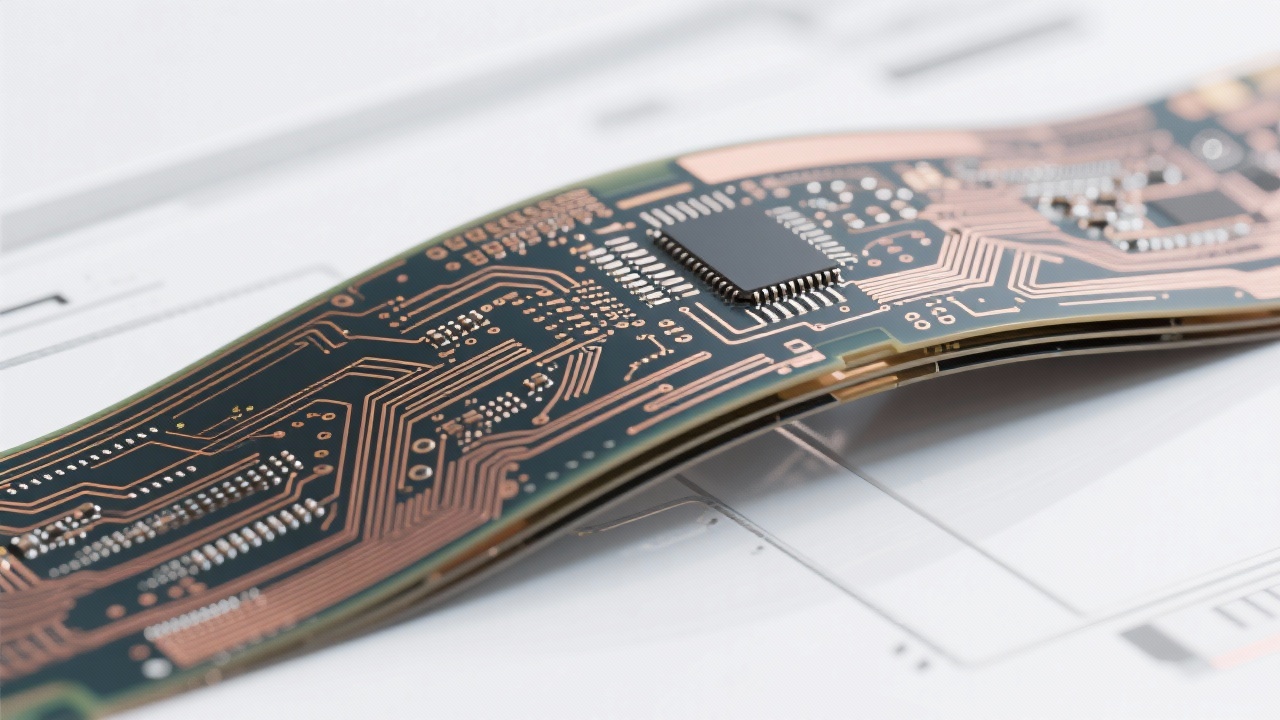
Regarding via design principles, the size and number of vias need to be carefully considered. Smaller vias can reduce the occupied area of the circuit board, while an appropriate number of vias can ensure good electrical connectivity. For instance, in a multi - layer FPC, the diameter of vias can be reduced to 0.1mm, which allows for more complex wiring designs.
Signal integrity is a major concern in FPC design. Signal crosstalk can cause signal distortion and affect the normal operation of the device. To address this issue, a variety of anti - crosstalk design strategies can be adopted. For example, using ground shields between signal lines can effectively reduce crosstalk. In a practical case of a medical monitoring device, by adding ground shields between critical signal lines, the crosstalk rate was reduced from 15% to less than 5%.

The optimization of electromagnetic compatibility (EMC) can improve the reliability of the device in different electromagnetic environments. Engineering practices have shown that by properly arranging the orientation and spacing of components, as well as using appropriate shielding materials, the EMC performance of FPCs can be significantly enhanced. For example, in some high - power electronic devices, through EMC optimization, the electromagnetic interference emission can be reduced by 30%.
Microhole processing technology is a key factor in realizing complex FPC structures. The smaller the minimum aperture of the microholes, the more complex wiring can be achieved on a limited - sized FPC. Currently, advanced manufacturing processes can achieve microhole diameters as small as 0.03mm, which greatly expands the design space for FPCs.
These advanced manufacturing capabilities not only support the production of FPCs with high - density wiring but also ensure the quality and reliability of the products. For example, in the production of smart wearable devices, the use of microhole processing technology allows for the integration of more functions on a small - sized FPC, meeting the requirements of miniaturization and high - performance of these devices.
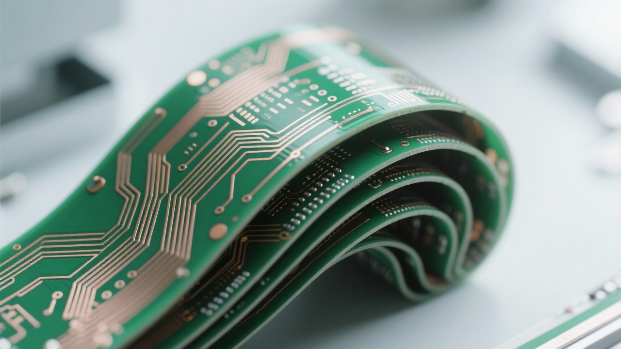
In consumer electronics, FPCs are widely used due to their flexibility and ability to meet the requirements of compact designs. For example, in foldable smartphones, FPCs with excellent folding performance are used to connect different parts of the device, enabling seamless folding and unfolding. In medical devices, FPCs are also crucial. They can be used in small - sized medical monitoring equipment, which needs to be lightweight and highly reliable.
The folding design and lightweight advantages of FPCs make them ideal for these applications. For instance, in some implantable medical devices, the use of FPCs can reduce the weight of the device by up to 40%, and the folding design allows the device to be more easily placed in the human body.
Our company adheres to strict industry certification standards to ensure the quality of FPC products. We have a professional R & D team and advanced production equipment, which can provide strong support for mass - production. Our products have passed a series of international certifications, such as ISO 9001, ensuring high - quality and stable production.
If you are looking for high - performance, reliable FPC solutions, our company can be your trusted partner. We are committed to collaborating with customers to provide the best technical support and product solutions. Explore our advanced FPC solutions now!
 358
|
358
|
 高密度柔性PCB设计
柔性电路板布局优化
FPC中的电磁兼容性
细间距PCB制造
消费电子产品柔性PCB
360
|
高密度FPC布线
柔性电路板设计
电磁兼容性优化
精密FPC制造
柔性PCB可靠性
412
|
双层PCB快速制造
PCB工艺流程
表面处理技术
飞针测试
PCB可靠性检测
96
|
FPC高密度布线
柔性电路板设计技术
电磁兼容性优化
高密度柔性PCB
多层FPC制造工艺
447
|
FPC高密度布线
柔性电路板设计技能
电磁兼容性优化
高密度柔性PCB
通过设计标准
高密度柔性PCB设计
柔性电路板布局优化
FPC中的电磁兼容性
细间距PCB制造
消费电子产品柔性PCB
360
|
高密度FPC布线
柔性电路板设计
电磁兼容性优化
精密FPC制造
柔性PCB可靠性
412
|
双层PCB快速制造
PCB工艺流程
表面处理技术
飞针测试
PCB可靠性检测
96
|
FPC高密度布线
柔性电路板设计技术
电磁兼容性优化
高密度柔性PCB
多层FPC制造工艺
447
|
FPC高密度布线
柔性电路板设计技能
电磁兼容性优化
高密度柔性PCB
通过设计标准
-4.png?x-oss-process=image/resize,h_800,m_lfit/format,webp)


-4.png?x-oss-process=image/resize,m_fill,h_800,w_800/format,webp)
-1.png?x-oss-process=image/resize,m_fill,h_800,w_800/format,webp)

