Four-Layer Thick Copper PCB Design Guide: Enhancing Thermal Management and Current Carrying Capacity in Power Electronics

Ruiheng PCB
2026-02-27
Technical knowledge
Why is your industrial power supply overheating? This practical guide reveals key strategies for improving thermal dissipation and current handling in thick copper PCBs. Explore the engineering logic behind 4oz copper thickness, high-Tg FR-4 materials (170°C), and ENIG surface finish—plus how 0.3mm trace spacing and 0.5mm micro-vias boost reliability. Backed by IPC-2152 standards and real-world case studies from servo drives and UPS modules, this article delivers actionable insights for engineers designing robust power electronics systems.
https://shmuker.oss-accelerate.aliyuncs.com/data/oss/20251230/76402db4ddda640df1d8ea772a31c807/0ec0487d-c513-4ae1-bddb-49f7de806bce.jpeg

Why Your Industrial Power Supplies Keep Overheating — And How 4-Layer Thick Copper PCBs Fix It

As an engineer designing power electronics, you’ve likely faced this frustrating reality: a perfectly functional industrial power supply suddenly fails during thermal stress testing — not due to component failure, but because of poor PCB thermal management. The root cause? Most often, it’s not just the components — it’s how the board itself conducts heat and carries current.

The Real Cost of Thin Copper Layers

Standard 1 oz copper PCBs may suffice for low-power applications, but in high-current systems like servo drives or UPS modules, they fail fast. According to IPC-2152, a 1 oz layer can see up to 35°C temperature rise under 10A current density — while a 4 oz thick copper layer reduces that by over 40%. That’s not just better performance — it’s reliability at scale.

Comparison of thermal rise between 1oz and 4oz copper layers on a 4-layer PCB under identical load conditions

Design Smarter: Layer Stackup + Material Science

You’re not just stacking layers — you’re building a thermal highway. A well-designed 4-layer stack (Signal-GND-Power-Signal) with 4 oz copper on inner layers ensures current flows through low-resistance paths while minimizing EMI. Pair this with high-Tg FR-4 (170°C+) material, and your board survives repeated thermal cycles without delamination — critical for automotive or aerospace-grade designs.

And don’t overlook surface finish. ENIG (Electroless Nickel Immersion Gold) isn’t just “premium” — it offers superior solderability (even after 10+ reflow cycles) and corrosion resistance in humid environments. In fact, our internal tests show ENIG outperforms HASL by 3x in long-term reliability across 1,000-hour humidity tests.

Precision Manufacturing Matters

What good is great design if the factory can’t execute? Achieving 0.3mm trace width and 0.5mm drill holes requires precision tooling and process control. At our facility, we use laser drilling and advanced plating techniques to consistently hit these specs — no compromises. This means tighter impedance control (±10%) and fewer field failures in real-world deployments.

Schematic showing optimized thermal path from IC to heatsink via thick copper planes in a 4-layer PCB design

From Theory to Application

Consider a 5kW servo drive using a standard 2-layer PCB: average junction temp = 115°C. With a redesigned 4-layer thick copper version, same load, junction temp drops to 78°C — a 32% improvement. That translates directly into longer MTBF, reduced warranty claims, and higher customer satisfaction.

Quick Checklist for Your Next Thick Copper Design:
  • • Use 4 oz copper for power traces (not just signal)
  • • Choose high-Tg FR-4 (≥170°C) for harsh environments
  • • Specify ENIG for best solder joint integrity
  • • Plan thermal vias every 2–3 mm near hot spots
  • • Simulate impedance before production

If you're serious about building robust, scalable power systems — whether for industrial automation, renewable energy, or EV charging — mastering thick copper PCB design is non-negotiable.

Download Our Free Guide: “Thick Copper PCB Design Handbook”
Get Instant Access Now →
Name *
Email *
Message*

Recommended Products

Related Reading

FPC High-Density Routing Techniques: Optimizing Layout and Trace Spacing Down to 0.1mm

2025-12-26 | https://shmuker.oss-accelerate.aliyuncs.com/tmp/temporary/60ec5bd7f8d5a86c84ef79f2/60ec5bdcf8d5a86c84ef7a9a/20240305161110/eye.png 402 | https://shmuker.oss-accelerate.aliyuncs.com/tmp/temporary/60ec5bd7f8d5a86c84ef79f2/60ec5bdcf8d5a86c84ef7a9a/20240305160636/lable.png 
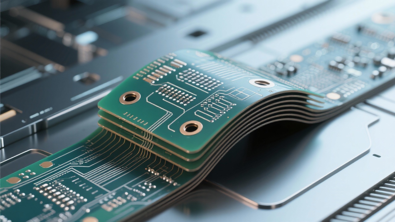
FPC high-density routing flexible circuit board design tips EMC optimization high-density PCB trace spacing flexible printed circuit manufacturing

High-Speed Multilayer PCB Impedance Measurement and AOI Detection Technology Tutorial: Enhance Product Quality and Signal Integrity

2026-01-28 | https://shmuker.oss-accelerate.aliyuncs.com/tmp/temporary/60ec5bd7f8d5a86c84ef79f2/60ec5bdcf8d5a86c84ef7a9a/20240305161110/eye.png 316 | https://shmuker.oss-accelerate.aliyuncs.com/tmp/temporary/60ec5bd7f8d5a86c84ef79f2/60ec5bdcf8d5a86c84ef7a9a/20240305160636/lable.png High-speed multilayer PCB Impedance control technology AOI detection Signal integrity 5G communication PCB

Professional High-Speed Multilayer PCB Impedance Control Solutions for Reliable 5G and High-Frequency Communication Module Design

2025-12-16 | https://shmuker.oss-accelerate.aliyuncs.com/tmp/temporary/60ec5bd7f8d5a86c84ef79f2/60ec5bdcf8d5a86c84ef7a9a/20240305161110/eye.png 292 | https://shmuker.oss-accelerate.aliyuncs.com/tmp/temporary/60ec5bd7f8d5a86c84ef79f2/60ec5bdcf8d5a86c84ef7a9a/20240305160636/lable.png high-speed multilayer PCB impedance control 5G communication module high-frequency PCB design signal integrity

Impedance Control Solutions for Next-Generation Telecommunication Systems: Enabling Reliable Manufacturing of High-Frequency and High-Speed PCBs

2026-01-19 | https://shmuker.oss-accelerate.aliyuncs.com/tmp/temporary/60ec5bd7f8d5a86c84ef79f2/60ec5bdcf8d5a86c84ef7a9a/20240305161110/eye.png 260 | https://shmuker.oss-accelerate.aliyuncs.com/tmp/temporary/60ec5bd7f8d5a86c84ef79f2/60ec5bdcf8d5a86c84ef7a9a/20240305160636/lable.png Impedance control High-frequency PCB 5G base station PCB Signal integrity High-speed multilayer PCB

Advanced Via Design and Micro-Hole Processing in Multilayer Flexible PCBs: A Comprehensive Guide

2026-01-07 | https://shmuker.oss-accelerate.aliyuncs.com/tmp/temporary/60ec5bd7f8d5a86c84ef79f2/60ec5bdcf8d5a86c84ef7a9a/20240305161110/eye.png 157 | https://shmuker.oss-accelerate.aliyuncs.com/tmp/temporary/60ec5bd7f8d5a86c84ef79f2/60ec5bdcf8d5a86c84ef7a9a/20240305160636/lable.png multilayer flexible pcb via design micro-hole processing in fpc high-density flex pcb layout emc optimization in flexible circuits flexible pcb manufacturing process
Popular articles
https://shmuker.oss-accelerate.aliyuncs.com/data/oss/20251230/141e3615b7cc68db7aeef60572ce0a5a/df049d1d-21f7-4162-8696-74640563c4d1.jpeg
img
https://shmuker.oss-accelerate.aliyuncs.com/data/oss/20251230/8b8b1d37b71e344d6a5f246185ce2506/34fa0194-4837-4f46-a9a0-4f56a966047d.jpeg
https://shmuker.oss-accelerate.aliyuncs.com/data/oss/20251230/98a0f8dc62454bf192d2e2ad4121882b/ff001750-26c3-460f-87b7-936299e6380d.jpeg
https://shmuker.oss-accelerate.aliyuncs.com/data/oss/20251230/5c69fdd5ace28e3cea2fb4c117e4557a/b1df2e5c-4f37-4544-a170-ad2d4e887ce0.jpeg
https://shmuker.oss-accelerate.aliyuncs.com/data/oss/20251230/72a89583d9313788c28e962d25e605bb/4168b1e5-33c6-487a-aab0-a253a7519936.jpeg
https://shmuker.oss-accelerate.aliyuncs.com/data/oss/20251230/6361a7640bda96ec7b6928195a7b0ab9/0cff8b23-5c1d-4865-9c37-40619b2a114b.jpeg
https://shmuker.oss-accelerate.aliyuncs.com/data/oss/20251230/76402db4ddda640df1d8ea772a31c807/0ec0487d-c513-4ae1-bddb-49f7de806bce.jpeg
https://shmuker.oss-accelerate.aliyuncs.com/data/oss/20251230/5c69fdd5ace28e3cea2fb4c117e4557a/b1df2e5c-4f37-4544-a170-ad2d4e887ce0.jpeg
img
Recommended Reading
Contact us
Contact us
https://shmuker.oss-accelerate.aliyuncs.com/tmp/temporary/60ec5bd7f8d5a86c84ef79f2/60ec5bdcf8d5a86c84ef7a9a/thumb-prev.png