
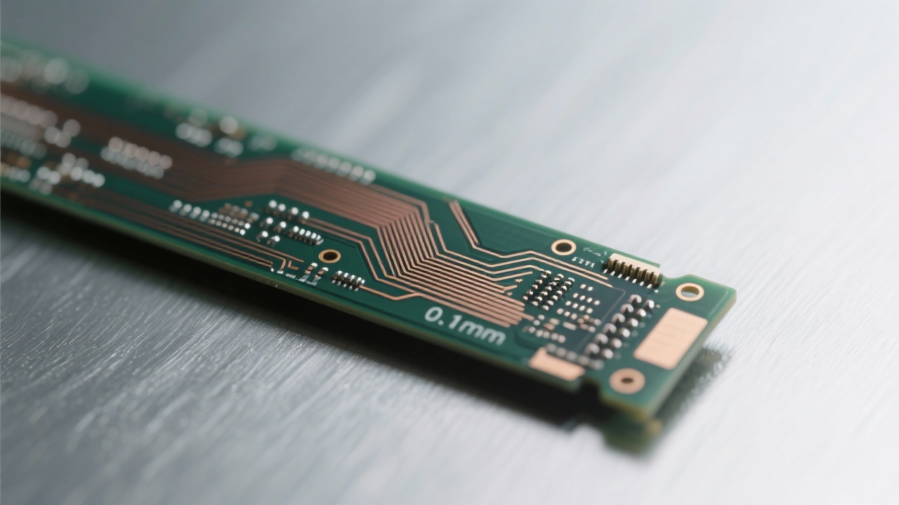
When designing high-reliability industrial power systems—such as motor drives, renewable energy inverters, or heavy-duty power supplies—engineers face a constant challenge: balancing thermal performance, current capacity, and signal integrity. A well-executed 4-layer thick copper PCB design is no longer optional—it’s essential for meeting today’s demanding specifications.
Standard 1-oz copper layers limit current handling to ~2A per 1mm trace under controlled conditions. In contrast, using 4 oz copper increases this by up to 4x—reaching over 8A per mm without overheating. This makes it ideal for applications like DC-DC converters where sustained load currents exceed 30A. The added thickness also reduces resistive losses (typically by 60–70%), which directly improves efficiency and minimizes hotspots on the board.
Industrial environments often expose PCBs to temperatures exceeding 125°C. Standard FR-4 materials can delaminate above 130°C, but high-Tg (≥170°C) versions maintain dimensional stability and dielectric strength even at peak loads. For example, a recent study by IPC found that boards using high-Tg FR-4 showed 3x fewer solder joint failures after 1000 thermal cycles compared to standard laminates.
Electroless Nickel Immersion Gold (ENIG) offers superior solderability, oxidation resistance, and planarity—critical for fine-pitch components used in modern power modules. It ensures consistent contact resistance (<0.5 mΩ), reducing voltage drop across connectors and minimizing EMI risks. Unlike HASL, ENIG doesn’t create uneven surfaces that could compromise BGA reflow quality.
Many engineers overlook key details like minimum trace spacing (at least 0.3mm for 4 oz copper) or fail to account for impedance control in multi-layer stacks. Without proper via placement and layer stackup planning, signal integrity degrades rapidly—even at 100 MHz. Use tools like Altium or Cadence to simulate parasitic effects before fabrication.
One common mistake? Ignoring thermal vias beneath power planes. Adding just 4–6 thermal vias per square inch can reduce hotspot temperatures by up to 15°C—a game-changer in enclosed enclosures.
A leading OEM in Europe redesigned their motor controller PCB using 4-layer thick copper, high-Tg FR-4, and ENIG finish. Post-implementation testing revealed:
Download our free Thick Copper PCB Design Handbook—packed with checklists, real-world examples, and industry-standard guidelines you won’t find elsewhere.
Get Your Free Design Guide Now → 463
|
463
|
 double-sided PCB manufacturing
surface treatment technologies
flying probe testing
PCB lamination process
rapid PCB delivery
220
|
FPC high - density routing
Flexible circuit board design techniques
Electromagnetic compatibility optimization
High - density routing solutions
Flexible PCB manufacturing processes
125
|
high-density FPC layout
flexible PCB design techniques
electromagnetic compatibility optimization
signal crosstalk prevention
advanced flexible PCB manufacturing
448
|
FPC high - density wiring
Flexible circuit board design skills
Electromagnetic compatibility optimization
High - density flexible PCB
Via design standards
157
|
multilayer flexible pcb via design
micro-hole processing in fpc
high-density flex pcb layout
emc optimization in flexible circuits
flexible pcb manufacturing process
double-sided PCB manufacturing
surface treatment technologies
flying probe testing
PCB lamination process
rapid PCB delivery
220
|
FPC high - density routing
Flexible circuit board design techniques
Electromagnetic compatibility optimization
High - density routing solutions
Flexible PCB manufacturing processes
125
|
high-density FPC layout
flexible PCB design techniques
electromagnetic compatibility optimization
signal crosstalk prevention
advanced flexible PCB manufacturing
448
|
FPC high - density wiring
Flexible circuit board design skills
Electromagnetic compatibility optimization
High - density flexible PCB
Via design standards
157
|
multilayer flexible pcb via design
micro-hole processing in fpc
high-density flex pcb layout
emc optimization in flexible circuits
flexible pcb manufacturing process


-4.png?x-oss-process=image/resize,m_fill,h_800,w_800/format,webp)
-L4-4.png?x-oss-process=image/resize,m_fill,h_800,w_800/format,webp)
-1.png?x-oss-process=image/resize,m_fill,h_800,w_800/format,webp)

