
Are frequent overheating issues plaguing your industrial power supply PCBs? Leveraging four-layer thick copper PCB designs can dramatically improve thermal dissipation and current carrying capacity. This guide dives into the pivotal role of 4 oz copper layers in power electronics, guiding you through material choice, structural layout, and manufacturing nuances to build more reliable, stable, and efficient power systems.
Copper thickness in PCBs directly affects both electrical and thermal performance. Thicker copper layers reduce resistance, limiting joule heating and improving current capacity. For instance, upgrading from 1 oz to 4 oz copper can boost current throughput by over 300%, while simultaneously lowering the temperature rise on your PCB by approximately 10-15°C under equivalent load conditions. However, blindly increasing copper thickness without other design considerations often leads to manufacturability challenges and diminishing returns.
A four-layer PCB stack-up typically combines signal and power layers to optimize space and functionality. Integrating thick copper layers (4 oz) on internal planes dedicated to power distribution enhances heat spreading efficiency, especially in high-current sections such as servodrivers or UPS modules.
Using a high Tg (glass transition temperature) FR-4 substrate with Tg around 170°C significantly improves your PCB’s reliability under elevated temperatures, preventing warping and delamination. This material choice is critical when your power device operates continuously in harsh thermal environments.
Electroless Nickel Immersion Gold (ENIG) surface treatment delivers superior solderability and excellent corrosion resistance, crucial for thick copper PCBs that experience frequent thermal cycling. ENIG minimizes the formation of brittle intermetallic compounds in solder joints, preserving mechanical integrity and extending the device lifespan.
Classic Pitfall Alert: Simply increasing copper thickness without adjusting trace width and spacing can lead to manufacturing defects and reliability issues. Follow IPC-2152 guidelines for current carrying capacity and maintain a minimum line spacing of 0.3 mm on 4 oz copper to prevent short circuits.
Also, consider thermal vias connecting thick copper planes to inner layers or heat sinks to maximize heat dissipation. This integrated thermal design approach significantly lowers hotspot formation, enhancing your device’s operational stability.
In servo drives, 4 oz copper layers along with high Tg FR-4 substrates ensure the controlled distribution of transient currents and reduce thermomechanical stress under rapid load changes. UPS modules benefit from enhanced copper thickness by maintaining continuous power delivery without overheating during peak loads, a key factor in preventing system failures.
Carefully evaluate your device’s thermal profile and mechanical constraints before finalizing the stack-up and materials. Leveraging published standards like IPC-2152 as design references will streamline your process and minimize costly reworks.
 358
|
358
|
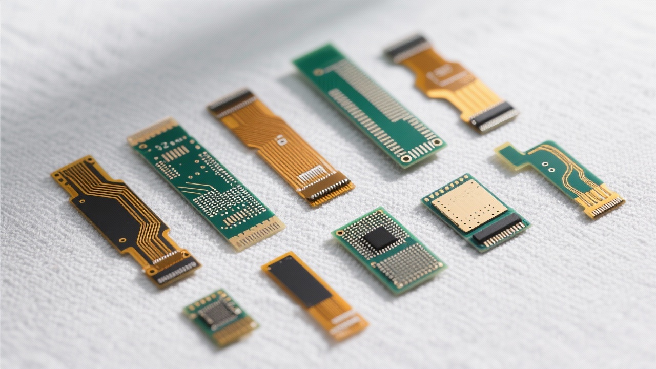
 high-density flexible PCB design
flexible circuit board layout optimization
electromagnetic compatibility in FPC
fine pitch PCB manufacturing
consumer electronics flexible PCB
410
|
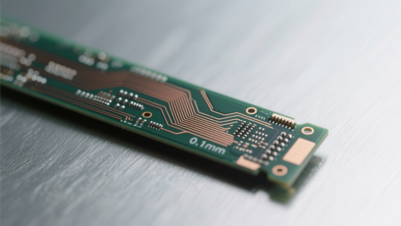
HDI PCB manufacturing
0.1 mm laser microvia
0.5 mm back drilling
IPC Class 3 via plating
semiconductor test PCB
152
|
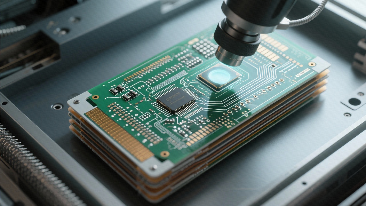
5G PCB design
impedance control
high-frequency communication modules
high-speed multilayer PCB
signal integrity
298
|
FPC high - density wiring
Flexible circuit board design skills
Electromagnetic compatibility optimization
Signal crosstalk protection
High - reliability FPC manufacturing
216
|
High-speed PCB impedance control
5G base station PCB design
High-frequency communication module impedance matching
High-performance dielectric material PCB
PCB signal integrity
high-density flexible PCB design
flexible circuit board layout optimization
electromagnetic compatibility in FPC
fine pitch PCB manufacturing
consumer electronics flexible PCB
410
|
HDI PCB manufacturing
0.1 mm laser microvia
0.5 mm back drilling
IPC Class 3 via plating
semiconductor test PCB
152
|
5G PCB design
impedance control
high-frequency communication modules
high-speed multilayer PCB
signal integrity
298
|
FPC high - density wiring
Flexible circuit board design skills
Electromagnetic compatibility optimization
Signal crosstalk protection
High - reliability FPC manufacturing
216
|
High-speed PCB impedance control
5G base station PCB design
High-frequency communication module impedance matching
High-performance dielectric material PCB
PCB signal integrity


-L4-4.png?x-oss-process=image/resize,m_fill,h_800,w_800/format,webp)


-4.png?x-oss-process=image/resize,m_fill,h_800,w_800/format,webp)