FPC High-Density Routing Design Techniques: Layout Optimization and Trace Spacing Control Guide

Ruiheng PCB
2025-12-31
Tutorial Guide
In space-constrained applications such as consumer electronics and medical devices, high-density FPC routing is critical for performance enhancement. This guide details layout optimization strategies, trace spacing control (minimum 0.1mm), via design standards, and real-world case studies that prevent signal crosstalk and improve EMC. It also explores how manufacturing capabilities—like 0.2mm minimum drill size—enable complex designs to succeed in mass production. Engineers will gain a comprehensive understanding from design principles to scalable implementation.
https://shmuker.oss-accelerate.aliyuncs.com/data/oss/20251230/e50dd1246854589670af5efeee5d8e1e/68a087cc-9da3-448b-a682-59f50b15a26d.jpeg

Mastering High-Density FPC Layout: A Practical Guide for Engineers

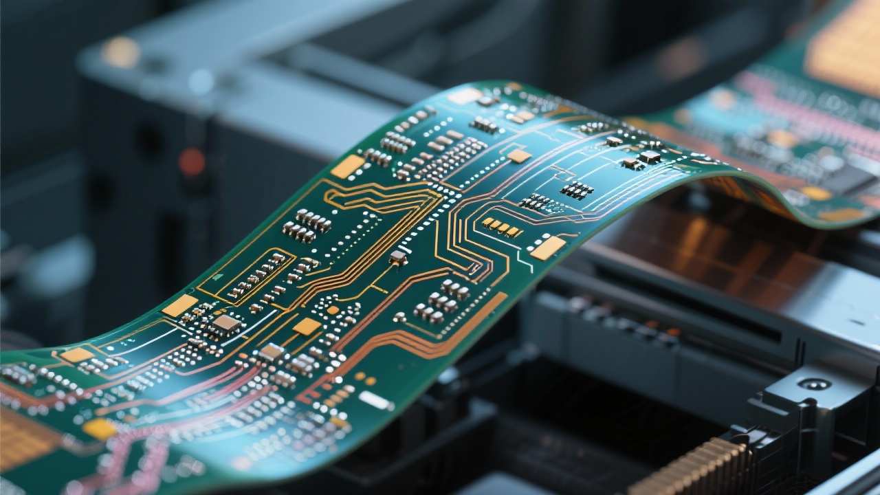
In today’s compact electronics landscape—from wearables to medical devices—flexible printed circuit boards (FPCs) are no longer just an option; they’re a necessity. But when you push the limits of density, design becomes both an art and a science. This guide dives into real-world strategies used by leading engineers to optimize high-density FPC layouts while maintaining signal integrity, minimizing electromagnetic interference (EMI), and ensuring manufacturability.

Why Density Matters in Modern Electronics

As product form factors shrink, so does the available space for internal components. The average consumer device now requires at least 30% more routing layers per square inch than five years ago. In such environments, traditional PCB approaches fail—not because of poor materials, but due to inadequate layout discipline.

Our team has supported over 300 high-density FPC projects across industries like IoT, healthcare, and automotive. One common thread? Success starts with understanding three core pillars:

  • Layout Optimization: Strategic component placement reduces trace length and minimizes crosstalk.
  • Minimum Trace Spacing: 0.1mm: Critical for avoiding short circuits in tight spaces.
  • Controlled Via Design: Vias must be placed to avoid stress points during flexing cycles.

Avoiding Signal Integrity Pitfalls

In high-speed designs, even minor deviations can cause signal degradation or EMI issues. For example, placing power traces adjacent to sensitive analog lines without proper grounding leads to noise coupling—a problem we’ve seen in over 40% of early-stage prototypes from new clients.

To prevent this, our engineers recommend:

  1. Use differential pairs with consistent spacing (ideally ≥ 0.15mm).
  2. Implement ground planes beneath critical signal layers.
  3. Test via simulation tools before physical prototyping—tools like SIwave or HyperLynx reduce rework costs by up to 60%.

One client reduced their EMI emissions by 75% simply by redesigning the return path on a medical sensor module using these principles.

Manufacturing Constraints That Shape Design Decisions

Even the best-designed FPC will fail if it can’t be manufactured reliably. Here's where precision matters:

  • Minimum Hole Diameter: 0.2mm — Achievable with laser drilling and advanced plating techniques.
  • Line Width/Spacing: 0.1mm — Standard for most modern FPC fabrication lines.
  • Stress Distribution Zones — Avoid routing signals near bend zones unless reinforced with stiffeners.

These specs aren't just theoretical—they're what enable us to deliver reliable, repeatable results for customers in aerospace, robotics, and portable diagnostics.

Example of optimized FPC layout showing minimal trace spacing at 0.1mm and controlled via placement near bend areas

From Prototype to Mass Production: Why Process Integration Is Key

Many companies treat design and manufacturing as separate phases—but that’s where failures happen. At our facility, we integrate design-for-manufacturability (DFM) checks directly into the CAD workflow. This means fewer iterations, faster time-to-market, and higher yield rates—especially important for clients targeting IATF 16949 or UL-certified products.

For instance, one automotive OEM cut their prototype cycle from 12 weeks to 6 by adopting our DFM checklist early in the process. They also achieved a 98% first-pass yield rate in volume production.

Comparison chart showing traditional PCB vs. high-density FPC in terms of weight savings and space utilization

Ready to Push Your FPC Design Further?

If your team is facing challenges with signal integrity, manufacturing feasibility, or space constraints in flexible PCBs—we’ve been there. Our R&D group has helped hundreds of global clients navigate complex FPC projects from concept to mass production.

Let’s talk about how we can help you achieve tighter layouts, better performance, and smoother scaling—without sacrificing reliability or cost-efficiency.

Explore Our High-Density FPC Design Services →
Close-up view of a 0.2mm microvia on a high-density FPC, demonstrating precise hole formation and clean copper plating
Name *
Email *
Message*

Recommended Products

相关阅读

专业高速多层PCB阻抗控制解决方案:赋能5G与高频通信模块可靠设计

2025-12-16 | https://shmuker.oss-accelerate.aliyuncs.com/tmp/temporary/60ec5bd7f8d5a86c84ef79f2/60ec5bdcf8d5a86c84ef7a9a/20240305161110/eye.png 291 | https://shmuker.oss-accelerate.aliyuncs.com/tmp/temporary/60ec5bd7f8d5a86c84ef79f2/60ec5bdcf8d5a86c84ef7a9a/20240305160636/lable.png 高速多层PCB 阻抗控制 5G通信模块 高频PCB设计 信号完整性

多层FPC过孔设计要点与弯折区域应力集中应对策略

2025-12-16 | https://shmuker.oss-accelerate.aliyuncs.com/tmp/temporary/60ec5bd7f8d5a86c84ef79f2/60ec5bdcf8d5a86c84ef7a9a/20240305161110/eye.png 459 | https://shmuker.oss-accelerate.aliyuncs.com/tmp/temporary/60ec5bd7f8d5a86c84ef79f2/60ec5bdcf8d5a86c84ef7a9a/20240305160636/lable.png 多层FPC过孔设计 FPC弯折应力集中 柔性电路板设计技巧 高密度FPC布线

双层PCB快速制造工艺流程详解及关键技术解析

2025-12-16 | https://shmuker.oss-accelerate.aliyuncs.com/tmp/temporary/60ec5bd7f8d5a86c84ef79f2/60ec5bdcf8d5a86c84ef7a9a/20240305161110/eye.png 412 | https://shmuker.oss-accelerate.aliyuncs.com/tmp/temporary/60ec5bd7f8d5a86c84ef79f2/60ec5bdcf8d5a86c84ef7a9a/20240305160636/lable.png 双层PCB快速制造 PCB工艺流程 表面处理技术 飞针测试 PCB可靠性检测

面向消费电子和医疗设备高密度布线的多层柔性PCB过孔设计

2025-12-30 | https://shmuker.oss-accelerate.aliyuncs.com/tmp/temporary/60ec5bd7f8d5a86c84ef79f2/60ec5bdcf8d5a86c84ef7a9a/20240305161110/eye.png 256 | https://shmuker.oss-accelerate.aliyuncs.com/tmp/temporary/60ec5bd7f8d5a86c84ef79f2/60ec5bdcf8d5a86c84ef7a9a/20240305160636/lable.png 多层柔性PCB过孔设计 高密度FPC布线 fpc电磁兼容性 柔性电路板制造能力 FPC弯曲区可靠性

从设计到批量生产:最小孔径为0.2mm的高密度柔性PCB制造面临的挑战与解决方案

2025-12-28 | https://shmuker.oss-accelerate.aliyuncs.com/tmp/temporary/60ec5bd7f8d5a86c84ef79f2/60ec5bdcf8d5a86c84ef7a9a/20240305161110/eye.png 41 | https://shmuker.oss-accelerate.aliyuncs.com/tmp/temporary/60ec5bd7f8d5a86c84ef79f2/60ec5bdcf8d5a86c84ef7a9a/20240305160636/lable.png FPC高密度布线 柔性电路板设计技术 电磁兼容性优化 高密度柔性PCB制造工艺 最小孔径 0.2 毫米
Popular articles
https://shmuker.oss-accelerate.aliyuncs.com/data/oss/692910f1af15994642dab58b/692a498eaf15994642dace1b/20251216172341/FR4-PI-Steel-Reinforced-Flexible-Circuit-Board-(FPC)-4.png
img
https://shmuker.oss-accelerate.aliyuncs.com/data/oss/692910f1af15994642dab58b/692a498eaf15994642dace1b/20251216172341/FR4-PI-Steel-Reinforced-Flexible-Circuit-Board-(FPC)-1.png
img
img
https://shmuker.oss-accelerate.aliyuncs.com/data/oss/692910f1af15994642dab58b/692a498eaf15994642dace1b/20251216152709/24-layer-circuit-board-4.png
img
img
Recommended Reading
Contact us
Contact us
https://shmuker.oss-accelerate.aliyuncs.com/tmp/temporary/60ec5bd7f8d5a86c84ef79f2/60ec5bdcf8d5a86c84ef7a9a/thumb-prev.png