FPC High-Density Routing: Key Techniques for Layout Optimization and Trace Spacing Control

Ruiheng PCB
2026-01-05
Technical knowledge
In high-density applications such as consumer electronics and medical devices, FPC routing design directly impacts product performance and reliability. This article explores critical techniques including layout optimization under spatial constraints, precise trace spacing control (as low as 0.1mm), via design strategies, bend zone stress management, and EMI mitigation. Real-world case studies demonstrate how to prevent signal crosstalk, enhance signal integrity, and leverage advanced manufacturing capabilities—such as 0.2mm minimum drill diameter—to realize complex designs. Engineers gain a comprehensive, end-to-end design logic from concept to mass production, supported by proven methodologies and practical insights.
https://shmuker.oss-accelerate.aliyuncs.com/data/oss/20251230/f546ee23d1f5b79cb30ea144c64bf7a0/41080766-f5fe-4275-980d-2f6b2674b30f.jpeg

Mastering High-Density FPC Routing: Precision Layouts and Signal Integrity

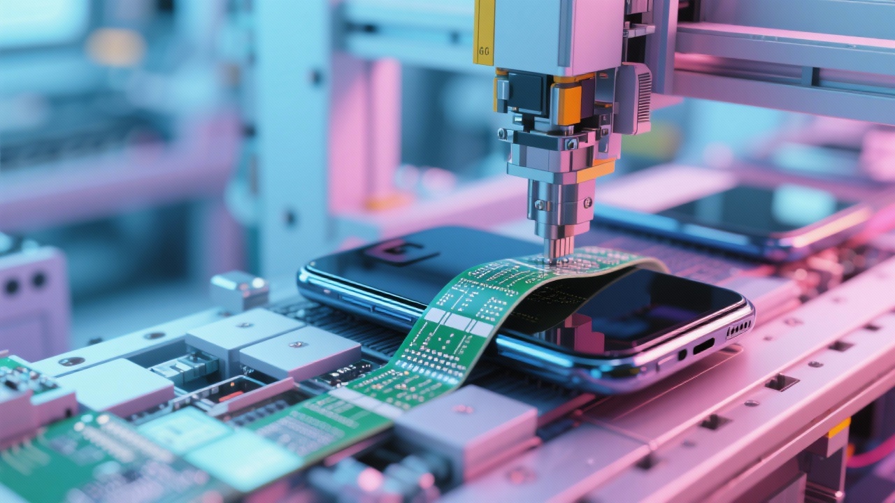
In today’s compact electronics—from wearables to medical devices—flexible printed circuits (FPCs) are pushing the limits of miniaturization. But with higher density comes greater complexity. The key to success? A systematic approach that balances design precision, manufacturability, and real-world performance.

Why Layout Optimization Matters More Than Ever

When space is at a premium, every millimeter counts. In high-density applications, designers often face trade-offs between signal routing efficiency and thermal management. For example, reducing trace spacing from 0.2mm to 0.1mm can increase component density by up to 40%, but it also demands tighter control over copper thickness, dielectric uniformity, and via placement. This isn’t just theoretical—it’s what we see in our clients’ projects daily.

Comparison chart showing signal integrity improvement when using optimized FPC layout vs traditional routing methods

Avoiding Signal Crosstalk: From Design to Manufacturing

Signal interference remains one of the top reasons for field failures in flexible PCBs. Our team has helped multiple OEMs reduce crosstalk by implementing ground plane shielding between critical signal layers and using staggered via patterns to minimize electromagnetic coupling. In one case, moving from a single-layer shield to a dual-layer isolation reduced EMI emissions by 62%—a result confirmed through lab testing using CISPR 11 standards.

What makes this possible? It starts with design rules that match manufacturing capabilities. At our facility, we consistently achieve 0.1mm line width and spacing, along with 0.2mm drill diameters—enabling complex multi-layer FPC designs that would otherwise be unfeasible.

Illustration of stress distribution in bend zones of an FPC, highlighting areas of high mechanical strain

Reliability Under Flex: Stress Management in Bend Regions

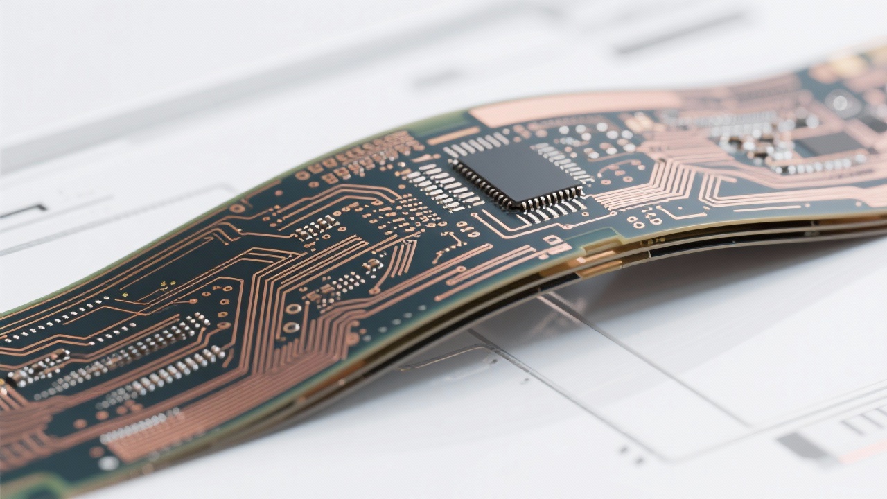
FPCs aren't static—they move. Whether it's a smartphone hinge or a surgical tool, repeated flexing creates localized stress points. Without proper design, these areas fail prematurely. We’ve developed a proprietary method combining material selection (polyimide vs. liquid crystal polymer), controlled bend radius (minimum 3mm), and reinforced copper plating to extend fatigue life by over 3x compared to standard approaches.

Our engineers don’t just design—they validate. Using finite element analysis (FEA), we simulate thousands of flex cycles before prototyping. That way, you get a product that works not just on paper, but in the real world.

You may have encountered similar challenges: tight tolerances, signal noise, or unexpected failures during prototype testing. What worked for us might work for you too.

Ready to Engineer Smarter?

We've delivered high-density FPC solutions to leading brands in healthcare, consumer tech, and industrial automation. Let’s discuss how we can support your next project—from concept to production.

Explore Our High-Density FPC Design Services
Name *
Email *
Message*

Recommended Products

相关阅读

先进的FPC制造技术:实现0.2mm最小过孔和高密度布线,适用于柔性电路

2026-01-04 | https://shmuker.oss-accelerate.aliyuncs.com/tmp/temporary/60ec5bd7f8d5a86c84ef79f2/60ec5bdcf8d5a86c84ef7a9a/20240305161110/eye.png 360 | https://shmuker.oss-accelerate.aliyuncs.com/tmp/temporary/60ec5bd7f8d5a86c84ef79f2/60ec5bdcf8d5a86c84ef7a9a/20240305160636/lable.png 高密度FPC布线 柔性电路板设计 电磁兼容性优化 精密FPC制造 柔性PCB可靠性

多层FPC过孔设计要点与弯折区域应力集中应对策略

2025-12-16 | https://shmuker.oss-accelerate.aliyuncs.com/tmp/temporary/60ec5bd7f8d5a86c84ef79f2/60ec5bdcf8d5a86c84ef7a9a/20240305161110/eye.png 459 | https://shmuker.oss-accelerate.aliyuncs.com/tmp/temporary/60ec5bd7f8d5a86c84ef79f2/60ec5bdcf8d5a86c84ef7a9a/20240305160636/lable.png 多层FPC过孔设计 FPC弯折应力集中 柔性电路板设计技巧 高密度FPC布线

双层PCB快速制造工艺流程详解及关键技术解析

2025-12-16 | https://shmuker.oss-accelerate.aliyuncs.com/tmp/temporary/60ec5bd7f8d5a86c84ef79f2/60ec5bdcf8d5a86c84ef7a9a/20240305161110/eye.png 412 | https://shmuker.oss-accelerate.aliyuncs.com/tmp/temporary/60ec5bd7f8d5a86c84ef79f2/60ec5bdcf8d5a86c84ef7a9a/20240305160636/lable.png 双层PCB快速制造 PCB工艺流程 表面处理技术 飞针测试 PCB可靠性检测

从设计到批量生产:最小孔径为0.2mm的高密度柔性PCB制造面临的挑战与解决方案

2025-12-28 | https://shmuker.oss-accelerate.aliyuncs.com/tmp/temporary/60ec5bd7f8d5a86c84ef79f2/60ec5bdcf8d5a86c84ef7a9a/20240305161110/eye.png 41 | https://shmuker.oss-accelerate.aliyuncs.com/tmp/temporary/60ec5bd7f8d5a86c84ef79f2/60ec5bdcf8d5a86c84ef7a9a/20240305160636/lable.png FPC高密度布线 柔性电路板设计技术 电磁兼容性优化 高密度柔性PCB制造工艺 最小孔径 0.2 毫米

多层柔性电路板高密度布线过孔设计挑战及制造工艺支持的研究

2026-01-02 | https://shmuker.oss-accelerate.aliyuncs.com/tmp/temporary/60ec5bd7f8d5a86c84ef79f2/60ec5bdcf8d5a86c84ef7a9a/20240305161110/eye.png 325 | https://shmuker.oss-accelerate.aliyuncs.com/tmp/temporary/60ec5bd7f8d5a86c84ef79f2/60ec5bdcf8d5a86c84ef7a9a/20240305160636/lable.png FPC高密度布线 柔性电路板设计技能 通过设计挑战 电磁兼容性优化 柔性PCB制造工艺
Populäre Artikel
img
https://shmuker.oss-accelerate.aliyuncs.com/data/oss/692910f1af15994642dab58b/692a498eaf15994642dace1b/20251216172341/FR4-PI-Steel-Reinforced-Flexible-Circuit-Board-(FPC)-1.png
https://shmuker.oss-accelerate.aliyuncs.com/data/oss/20251230/e50dd1246854589670af5efeee5d8e1e/68a087cc-9da3-448b-a682-59f50b15a26d.jpeg
https://shmuker.oss-accelerate.aliyuncs.com/data/oss/20251230/d47ffe47fe3f2d0fde94b14a5ca4b52e/aa681be2-e9be-4c8a-a019-f33ba92e2899.jpeg
https://shmuker.oss-accelerate.aliyuncs.com/data/oss/20251230/f546ee23d1f5b79cb30ea144c64bf7a0/41080766-f5fe-4275-980d-2f6b2674b30f.jpeg
https://shmuker.oss-accelerate.aliyuncs.com/data/oss/20251230/ad1efdc43fb7ec87673b41226508fc2d/ca4a2711-4cda-4529-a7a3-1efe9c8f1ada.jpeg
https://shmuker.oss-accelerate.aliyuncs.com/data/oss/692910f1af15994642dab58b/692a498eaf15994642dace1b/20251216152709/24-layer-circuit-board-4.png
img
https://shmuker.oss-accelerate.aliyuncs.com/data/oss/20251230/10162eed1c55dc9d2c2f47a0acfd4f76/514a91c4-e6c4-488d-a6e8-0a112d4b66b7.jpeg
img
推荐阅读
Contact us
Contact us
https://shmuker.oss-accelerate.aliyuncs.com/tmp/temporary/60ec5bd7f8d5a86c84ef79f2/60ec5bdcf8d5a86c84ef7a9a/thumb-prev.png