
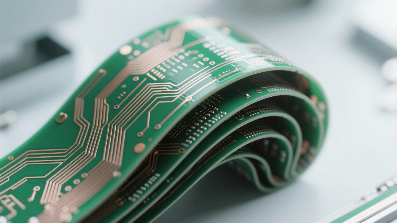
In high - density application scenarios such as consumer electronics and medical devices, the trace spacing and via design of Flexible Printed Circuits (FPC) directly determine signal integrity and product reliability. This article delves deep into the technical standards and engineering practices of a minimum line width/spacing of 0.1mm and a 0.2mm micro - via process.
High - density FPC design is fraught with challenges. There are three core difficulties: layout optimization strategies, methods for controlling trace spacing (including the path to achieving a minimum of 0.1mm), and the selection of via types and management of stress distribution. For example, when it comes to trace spacing, achieving a minimum of 0.1mm requires a high - precision manufacturing process. By referring to industry standards like IPC - 2221 and real - world project cases, we can understand how to reduce the risk of signal crosstalk through design simulation and process matching. Through simulation, engineers can predict the impact of different trace spacings and via types on signal transmission, and then adjust the design accordingly.
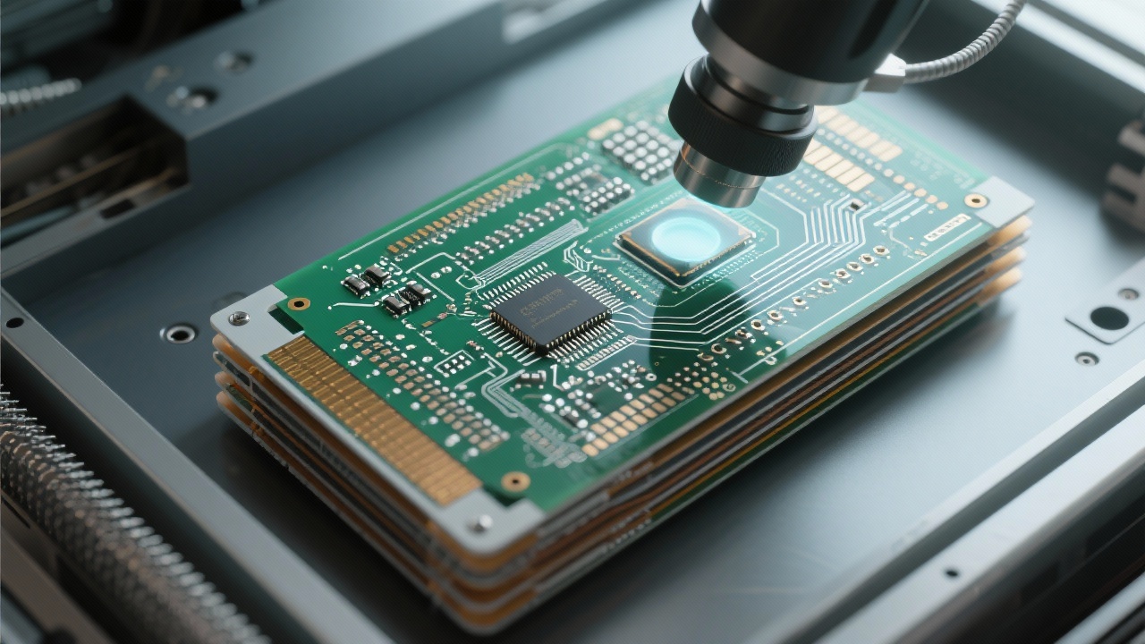
The manufacturing end plays a crucial role in supporting high - precision requirements. Laser drilling accuracy is a key factor. With advanced laser drilling technology, it is possible to achieve a minimum aperture of 0.2mm, which is essential for high - density FPCs. Copper foil treatment technology also affects the performance of FPCs. Proper treatment can improve the conductivity and stability of the circuit. In addition, strengthening solutions for bending areas are necessary. For instance, using special materials or structures in bending areas can enhance the durability of the FPC.
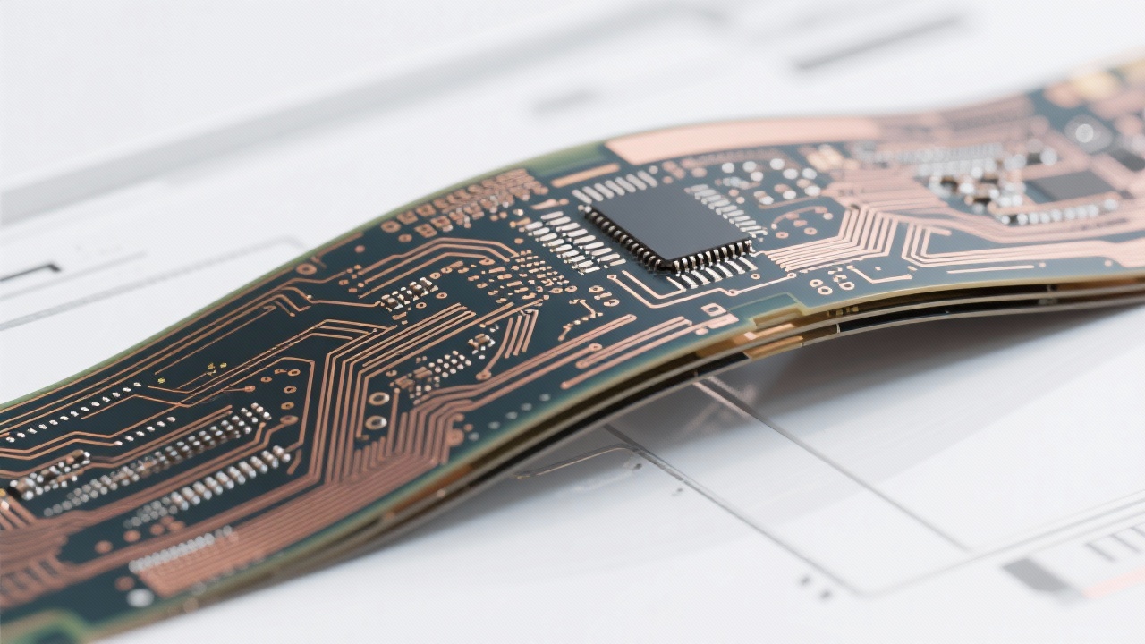
Typical failure scenarios, such as fractures in bending areas and excessive Electromagnetic Compatibility (EMC) levels, are common in FPC applications. By conducting an in - depth analysis of these failure scenarios, we can find the root causes and provide preventive measures. For example, fractures in bending areas may be due to improper stress distribution or the use of low - quality materials. To prevent this, we can optimize the via design and strengthen the bending areas. For EMC issues, we can optimize the trace spacing and via types to improve electromagnetic compatibility.
We understand the importance of a one - stop solution from R & D to mass production. We have already helped multiple high - end customers achieve the implementation of such designs. Our team can provide support throughout the entire process, from design to manufacturing. This not only saves time and cost for customers but also ensures the quality and reliability of the products.
In conclusion, mastering the core points of high - density FPC from design to mass production is essential for engineers. By understanding the technical standards, manufacturing capabilities, and preventive measures for failure scenarios, engineers can create high - quality FPC products. If you want to learn more about high - density FPC design and manufacturing, click here to explore our solutions.
 360
|
360
|
 High-density FPC routing
Flexible circuit board design
Electromagnetic compatibility optimization
Precision FPC manufacturing
Flexible PCB reliability
125
|
high-density FPC layout
flexible PCB design techniques
electromagnetic compatibility optimization
signal crosstalk prevention
advanced flexible PCB manufacturing
459
|
Multilayer FPC Via Design
FPC Bend Area Stress
Flexible Circuit Design
High-Density FPC Routing
FPC Reliability Enhancement
317
|
high-density FPC routing
flexible PCB design
EMI optimization
medical FPC
consumer electronics FPC
325
|
FPC high - density wiring
Flexible circuit board design skills
Via design challenges
Electromagnetic compatibility optimization
Flexible PCB manufacturing process
High-density FPC routing
Flexible circuit board design
Electromagnetic compatibility optimization
Precision FPC manufacturing
Flexible PCB reliability
125
|
high-density FPC layout
flexible PCB design techniques
electromagnetic compatibility optimization
signal crosstalk prevention
advanced flexible PCB manufacturing
459
|
Multilayer FPC Via Design
FPC Bend Area Stress
Flexible Circuit Design
High-Density FPC Routing
FPC Reliability Enhancement
317
|
high-density FPC routing
flexible PCB design
EMI optimization
medical FPC
consumer electronics FPC
325
|
FPC high - density wiring
Flexible circuit board design skills
Via design challenges
Electromagnetic compatibility optimization
Flexible PCB manufacturing process


-L4-4.png?x-oss-process=image/resize,m_fill,h_800,w_800/format,webp)


-4.png?x-oss-process=image/resize,m_fill,h_800,w_800/format,webp)
-1.png?x-oss-process=image/resize,h_800,m_lfit/format,webp)


