High-Density Flexible Circuit Board Design Challenges and Manufacturing Process Innovations Boost Product Reliability

Ruiheng PCB
2026-01-08
Special report
This article delves into the key technologies of high-density wiring in flexible printed circuit board (FPC) design and manufacturing process innovations. It focuses on analyzing the design challenges of single-sided, double-sided, and multi-layer FPCs in layout optimization, minimum trace spacing (0.1mm), via design, and signal integrity assurance. Through practical application cases in space-sensitive fields such as consumer electronics and medical devices, it reveals how to effectively avoid signal crosstalk and improve electromagnetic compatibility, and proposes reliability improvement solutions for the problem of bending stress concentration. The article also specifically introduces how the precision machining technology on the manufacturing side (minimum hole diameter of 0.2mm) supports the mass production implementation of complex high-density designs, providing engineers with a full-process guide from design principles to production processes. The content combines industry standards and the latest technologies, integrates practical cases and soft product recommendations, aiming to help professional readers comprehensively master the technical context of high-density flexible PCB design and promote the improvement of product performance and reliability.
https://shmuker.oss-accelerate.aliyuncs.com/data/oss/20251230/74cae3ecdb9a0b7f18e44f6631cea9fa/a50611de-8ff5-4f46-a7e1-6a2a52b90b99.jpeg

Challenges in High - Density Flexible Circuit Board Design and Manufacturing Process Innovation for Product Reliability Enhancement

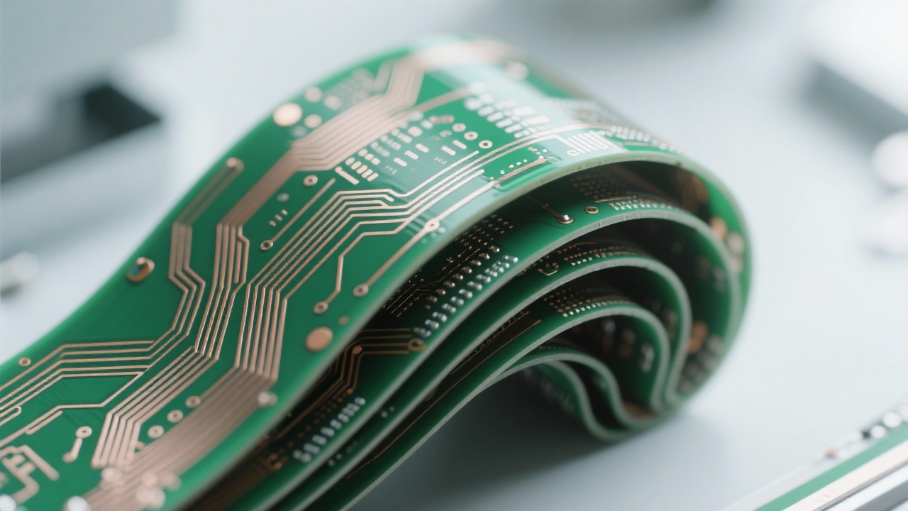
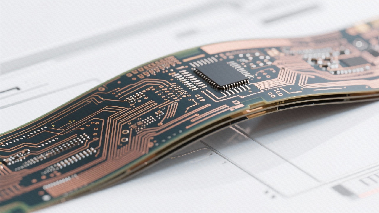
In the era of rapid technological development, high - density flexible printed circuit boards (FPCs) have become a key component in various industries, especially in space - sensitive fields such as consumer electronics and medical devices. This article delves deep into the core technical difficulties in high - density FPC design and manufacturing process innovation.

Key Design Parameters in High - Density FPC

Layout optimization, trace spacing control, and via design are crucial aspects in high - density FPC design. For single - sided, double - sided, and multi - layer FPCs, designers face significant challenges in achieving the best layout. The minimum trace spacing is set at 0.1mm, which requires precise control during the design process. Via design also plays a vital role in ensuring signal integrity. For example, improper via design can lead to signal loss and electromagnetic interference.

配图_1767066646481.jpg

Design Challenges and Solutions

In high - density FPC design, signal crosstalk and electromagnetic compatibility are major concerns. In space - sensitive applications like consumer electronics and medical devices, signal crosstalk can seriously affect the performance of the entire system. To address this issue, designers need to optimize the layout and use appropriate shielding techniques. By referring to real - world application cases in these industries, we can see how effective layout optimization can reduce signal crosstalk and improve electromagnetic compatibility.

Another problem is the stress concentration during bending. Flexible circuit boards often need to be bent during use, and stress concentration can lead to cracks and reduced reliability. Our article provides solutions to enhance the reliability of FPCs under bending conditions, such as using special materials and structural designs.

配图_1767066611257.jpg

Manufacturing Process Innovation

On the manufacturing side, precision processing technologies are essential for mass - producing complex high - density designs. The minimum hole diameter is 0.2mm, which requires high - precision drilling and other processing techniques. These advanced manufacturing technologies support the implementation of complex high - density designs, ensuring that the designed products can be mass - produced with high quality.

This article combines industry standards and the latest technologies, integrating practical cases and product recommendations. It aims to provide engineers with a comprehensive guide from design principles to production processes, helping them fully master the technical framework of high - density flexible PCB design and promote the improvement of product performance and reliability.

配图_1767066641679.jpg

If you are an engineer or a professional in the field of flexible circuit boards, and you want to learn more about high - density FPC design and manufacturing, click here to explore our in - depth solutions and take your product to the next level!

Name *
Email *
Message*

Recommended Products

Related Reading

Enhancing Consumer Electronics Performance with High-Density Flexible PCB Design

2026-01-03 | https://shmuker.oss-accelerate.aliyuncs.com/tmp/temporary/60ec5bd7f8d5a86c84ef79f2/60ec5bdcf8d5a86c84ef7a9a/20240305161110/eye.png 358 | https://shmuker.oss-accelerate.aliyuncs.com/tmp/temporary/60ec5bd7f8d5a86c84ef79f2/60ec5bdcf8d5a86c84ef7a9a/20240305160636/lable.png high-density flexible PCB design flexible circuit board layout optimization electromagnetic compatibility in FPC fine pitch PCB manufacturing consumer electronics flexible PCB

Optimizing EMI and Signal Integrity in High-Density Flexible PCB Design: Case Studies and Manufacturing Insights

2026-01-01 | https://shmuker.oss-accelerate.aliyuncs.com/tmp/temporary/60ec5bd7f8d5a86c84ef79f2/60ec5bdcf8d5a86c84ef7a9a/20240305161110/eye.png 159 | https://shmuker.oss-accelerate.aliyuncs.com/tmp/temporary/60ec5bd7f8d5a86c84ef79f2/60ec5bdcf8d5a86c84ef7a9a/20240305160636/lable.png high-density FPC design flexible PCB signal integrity EMI optimization in FPC signal crosstalk prevention microvia fabrication in flexible PCB

From Design to Mass Production: Challenges and Solutions in High-Density Flexible PCB Manufacturing with a Minimum Hole Diameter of 0.2mm

2025-12-28 | https://shmuker.oss-accelerate.aliyuncs.com/tmp/temporary/60ec5bd7f8d5a86c84ef79f2/60ec5bdcf8d5a86c84ef7a9a/20240305161110/eye.png 41 | https://shmuker.oss-accelerate.aliyuncs.com/tmp/temporary/60ec5bd7f8d5a86c84ef79f2/60ec5bdcf8d5a86c84ef7a9a/20240305160636/lable.png FPC high-density wiring Flexible circuit board design techniques Electromagnetic compatibility optimization High-density flexible PCB manufacturing process Minimum hole diameter 0.2mm

Research on Via Design Challenges and Manufacturing Process Support in High-Density Wiring of Multi-Layer Flexible Circuit Boards

2026-01-02 | https://shmuker.oss-accelerate.aliyuncs.com/tmp/temporary/60ec5bd7f8d5a86c84ef79f2/60ec5bdcf8d5a86c84ef7a9a/20240305161110/eye.png 325 | https://shmuker.oss-accelerate.aliyuncs.com/tmp/temporary/60ec5bd7f8d5a86c84ef79f2/60ec5bdcf8d5a86c84ef7a9a/20240305160636/lable.png FPC high - density wiring Flexible circuit board design skills Via design challenges Electromagnetic compatibility optimization Flexible PCB manufacturing process

Advanced Via Design and Micro-Hole Processing in Multilayer Flexible PCBs: A Comprehensive Guide

2026-01-07 | https://shmuker.oss-accelerate.aliyuncs.com/tmp/temporary/60ec5bd7f8d5a86c84ef79f2/60ec5bdcf8d5a86c84ef7a9a/20240305161110/eye.png 156 | https://shmuker.oss-accelerate.aliyuncs.com/tmp/temporary/60ec5bd7f8d5a86c84ef79f2/60ec5bdcf8d5a86c84ef7a9a/20240305160636/lable.png multilayer flexible pcb via design micro-hole processing in fpc high-density flex pcb layout emc optimization in flexible circuits flexible pcb manufacturing process
Popular articles
https://shmuker.oss-accelerate.aliyuncs.com/data/oss/692910f1af15994642dab58b/692a498eaf15994642dace1b/20251216172341/FR4-PI-Steel-Reinforced-Flexible-Circuit-Board-(FPC)-4.png
img
https://shmuker.oss-accelerate.aliyuncs.com/data/oss/20251230/d47ffe47fe3f2d0fde94b14a5ca4b52e/aa681be2-e9be-4c8a-a019-f33ba92e2899.jpeg
https://shmuker.oss-accelerate.aliyuncs.com/data/oss/20251230/f546ee23d1f5b79cb30ea144c64bf7a0/41080766-f5fe-4275-980d-2f6b2674b30f.jpeg
https://shmuker.oss-accelerate.aliyuncs.com/data/oss/20251230/ad1efdc43fb7ec87673b41226508fc2d/ca4a2711-4cda-4529-a7a3-1efe9c8f1ada.jpeg
img
https://shmuker.oss-accelerate.aliyuncs.com/data/oss/20251230/f546ee23d1f5b79cb30ea144c64bf7a0/41080766-f5fe-4275-980d-2f6b2674b30f.jpeg
https://shmuker.oss-accelerate.aliyuncs.com/data/oss/20251230/5c69fdd5ace28e3cea2fb4c117e4557a/b1df2e5c-4f37-4544-a170-ad2d4e887ce0.jpeg
https://shmuker.oss-accelerate.aliyuncs.com/data/oss/20251230/72a89583d9313788c28e962d25e605bb/4168b1e5-33c6-487a-aab0-a253a7519936.jpeg
img
Recommended Reading
Contact us
Contact us
https://shmuker.oss-accelerate.aliyuncs.com/tmp/temporary/60ec5bd7f8d5a86c84ef79f2/60ec5bdcf8d5a86c84ef7a9a/thumb-prev.png