
In the rapidly evolving consumer electronics sector, the demand for compact, high-performance devices necessitates advanced electronic components, particularly Flexible Printed Circuits (FPC). This article dives into the technical nuances of high-density flexible PCB design, reflecting on industry best practices and a detailed client case from the consumer electronics domain. It underscores how meticulous design and manufacturing processes improve signal integrity, reduce electromagnetic interference, and boost overall product reliability.
High-density flex PCB design imposes stringent requirements on layout optimization, ultra-fine trace routing, and via technologies. Key challenges stem from minimizing trace width and spacing — often pushing to line widths and spaces as narrow as 0.1mm — and maintaining structural integrity in multilayer boards. Effective layout optimization involves:
Precise control of line width and spacing is critical to reduce signal attenuation and electromagnetic interference (EMI). Industry standards like IPC-2223B provide guidelines for flexible PCB designs, ensuring manufacturability without compromising electrical performance.
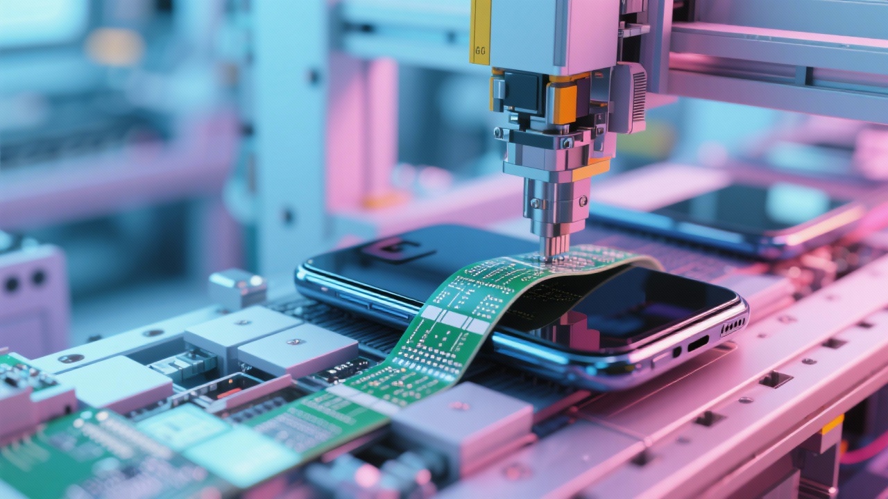
A leading consumer electronics manufacturer collaborated with a flexible PCB supplier to develop an ultra-thin wearable device requiring high-density FPC with multilayer flexibility. The primary obstacles included controlling signal crosstalk in dense routing environments and ensuring robust electromagnetic compatibility (EMC).
The project employed advanced simulation tools during the design phase to model electromagnetic fields and signal propagation. This allowed precise adjustment of trace spacing and shielding layers within the multi-layer FPC stack, achieving over 30% reduction in signal noise compared to prior designs.
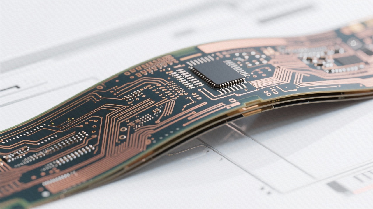
Structural reliability was enhanced by applying durable coverlay materials and tailoring bend radii based on fatigue analyses to withstand repeated flexing in dynamic usage scenarios.

Precision manufacturing capabilities are pivotal to realizing intricate designs. The selected manufacturer leveraged cutting-edge photolithography and laser drilling techniques to achieve minimum hole diameters of 0.2 mm and line widths/spacing down to 0.1 mm. These processes enable multilayer flexible PCBs with consistent electrical performance and mechanical endurance.
Furthermore, advanced lamination and bonding processes allow integration of foldable and stackable features, expanding the product’s spatial efficiency without sacrificing reliability.
Engineers aiming to elevate their designs with high-density flexible PCBs should consider the following:
Integrating these strategies fosters a holistic approach from conceptual design to mass production, ensuring devices perform reliably in space-constrained consumer electronics applications.
 291
|
291
|
 high-speed multilayer PCB
impedance control
5G communication module
high-frequency PCB design
signal integrity
459
|
Multilayer FPC Via Design
FPC Bend Area Stress
Flexible Circuit Design
High-Density FPC Routing
FPC Reliability Enhancement
412
|
double layer PCB rapid manufacturing
PCB surface finishing technologies
flying probe testing
PCB production process
electrical reliability testing
41
|
FPC high-density wiring
Flexible circuit board design techniques
Electromagnetic compatibility optimization
High-density flexible PCB manufacturing process
Minimum hole diameter 0.2mm
325
|
FPC high - density wiring
Flexible circuit board design skills
Via design challenges
Electromagnetic compatibility optimization
Flexible PCB manufacturing process
high-speed multilayer PCB
impedance control
5G communication module
high-frequency PCB design
signal integrity
459
|
Multilayer FPC Via Design
FPC Bend Area Stress
Flexible Circuit Design
High-Density FPC Routing
FPC Reliability Enhancement
412
|
double layer PCB rapid manufacturing
PCB surface finishing technologies
flying probe testing
PCB production process
electrical reliability testing
41
|
FPC high-density wiring
Flexible circuit board design techniques
Electromagnetic compatibility optimization
High-density flexible PCB manufacturing process
Minimum hole diameter 0.2mm
325
|
FPC high - density wiring
Flexible circuit board design skills
Via design challenges
Electromagnetic compatibility optimization
Flexible PCB manufacturing process
-4.png?x-oss-process=image/resize,h_800,m_lfit/format,webp)

-1.png?x-oss-process=image/resize,h_800,m_lfit/format,webp)


-4.png?x-oss-process=image/resize,m_fill,h_800,w_800/format,webp)
-1.png?x-oss-process=image/resize,m_fill,h_800,w_800/format,webp)

-L4-4.png?x-oss-process=image/resize,m_fill,h_800,w_800/format,webp)
