
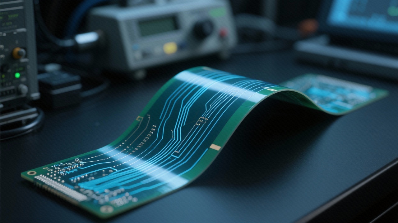
As consumer electronics and medical devices push toward miniaturization, flexible printed circuit boards (FPCs) have become essential for achieving high-density layouts without compromising signal integrity. But with increased complexity comes new challenges—especially in electromagnetic compatibility (EMC) and signal crosstalk prevention.
In applications like wearables, endoscopes, or IoT sensors, even minor EMI can cause system failures or regulatory non-compliance. According to IPC-2152 standards, maintaining a minimum spacing of 0.2mm between traces helps reduce crosstalk by up to 60% in high-frequency designs (above 5 GHz). This isn’t just theory—it’s validated through real-world testing at our R&D lab, where we simulate conditions mimicking actual field use.
For example, one client designing a smartwatch PCB faced intermittent Bluetooth dropouts during prototype testing. After reviewing their layout, we identified that adjacent signal layers were too close (<0.15mm), causing excessive coupling. By increasing trace separation to 0.25mm and adding ground planes between sensitive lines, the issue vanished—a change that saved weeks of rework and ensured compliance with FCC Part 15 Class B emissions limits.
High-density FPC design isn't complete without manufacturing capabilities that match the engineering intent. Our facility supports microvia drilling down to 0.2mm diameter and line widths/spacing as fine as 0.1mm—critical for modern mobile and medical-grade boards. These specs aren’t just marketing claims; they’re backed by consistent yield rates above 97% across thousands of production runs.
When designers specify tight tolerances, it's vital that fabrication partners understand how these affect performance. For instance, poor via plating quality in small holes can increase impedance mismatch by up to 15%, leading to signal reflection issues. That’s why we invest heavily in automated optical inspection (AOI) systems and real-time process monitoring to ensure every board meets both electrical and mechanical requirements.
The synergy between smart design and precise manufacturing is what sets reliable FPCs apart from those that fail under stress. Whether you're working on a compact hearing aid or an automotive sensor module, getting this balance right means fewer redesigns, faster time-to-market, and stronger customer trust.
If your team struggles with signal integrity or EMC compliance in flexible PCBs, consider downloading our free “High-Density FPC Design Checklist”—a practical guide developed by our senior engineers based on over 100 successful projects. It includes best practices for routing, via placement, and layer stackup optimization tailored for space-constrained environments.
And if you'd like to see how our advanced manufacturing process handles your specific design challenge, schedule a quick technical consultation—we’ll review your Gerber files and provide actionable feedback within 48 hours.
 291
|
291
|
 high-speed multilayer PCB
impedance control
5G communication module
high-frequency PCB design
signal integrity
459
|
Multilayer FPC Via Design
FPC Bend Area Stress
Flexible Circuit Design
High-Density FPC Routing
FPC Reliability Enhancement
412
|
double layer PCB rapid manufacturing
PCB surface finishing technologies
flying probe testing
PCB production process
electrical reliability testing
256
|
multilayer flexible pcb via design
high-density fpc routing
fpc electromagnetic compatibility
flexible circuit board manufacturing capability
fpc bend zone reliability
377
|
FPC high-density routing
flexible PCB design
trace spacing control
high-density PCB manufacturing
electromagnetic compatibility
high-speed multilayer PCB
impedance control
5G communication module
high-frequency PCB design
signal integrity
459
|
Multilayer FPC Via Design
FPC Bend Area Stress
Flexible Circuit Design
High-Density FPC Routing
FPC Reliability Enhancement
412
|
double layer PCB rapid manufacturing
PCB surface finishing technologies
flying probe testing
PCB production process
electrical reliability testing
256
|
multilayer flexible pcb via design
high-density fpc routing
fpc electromagnetic compatibility
flexible circuit board manufacturing capability
fpc bend zone reliability
377
|
FPC high-density routing
flexible PCB design
trace spacing control
high-density PCB manufacturing
electromagnetic compatibility
-4.png?x-oss-process=image/resize,h_800,m_lfit/format,webp)

-1.png?x-oss-process=image/resize,h_800,m_lfit/format,webp)


-L4-4.png?x-oss-process=image/resize,m_fill,h_800,w_800/format,webp)
-4.png?x-oss-process=image/resize,m_fill,h_800,w_800/format,webp)