Mastering High-Density Routing in FPC Design: Techniques for Optimized Layout and Signal Integrity

Ruiheng PCB
2026-01-10
Tutorial Guide
This article explores key strategies for achieving high-density routing in flexible printed circuit boards (FPCs), addressing design challenges across single-layer, double-layer, and multilayer configurations. It covers layout optimization, minimum trace spacing of 0.1mm, via design considerations—including 0.2mm hole diameter capabilities—and real-world solutions to signal crosstalk, EMI issues, and stress concentration at bend zones. Supported by industry standards and practical case studies, this guide highlights advanced manufacturing processes that enable precision fabrication. Learn how to enhance reliability, reduce design iteration, and accelerate time-to-market—backed by proven methodologies and scalable production support from a trusted FPC provider.
https://shmuker.oss-accelerate.aliyuncs.com/data/oss/20251230/5c69fdd5ace28e3cea2fb4c117e4557a/b1df2e5c-4f37-4544-a170-ad2d4e887ce0.jpeg

Mastering High-Density FPC Layout: Practical Tips for Reliable Flexible Circuit Design

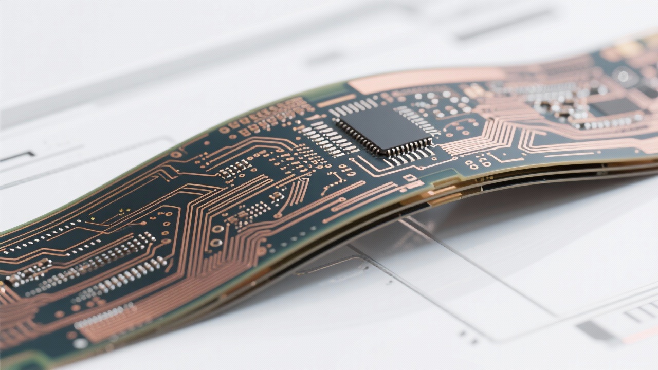
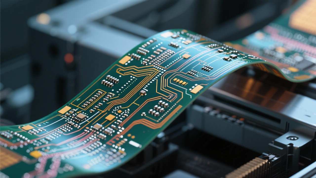
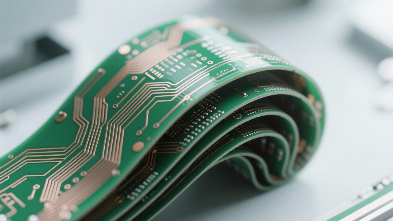
In today’s compact electronics landscape—from wearables to automotive sensors—flexible printed circuits (FPCs) are no longer optional. They’re essential. But achieving high-density routing without compromising reliability? That’s where many engineers struggle.

Why Density Matters in Modern FPC Design

With devices shrinking and functionality increasing, designers must push line widths and spacing down to 0.1mm or less—a feat only possible with advanced manufacturing capabilities. According to IPC-2221 standards, this level of precision demands tighter tolerances in both design and production. Ignoring these limits leads to signal crosstalk, EMI issues, and mechanical failure at bend points.

Key Strategies for Optimizing FPC Layouts

  • Single vs. Double vs. Multi-Layer Designs: Single-layer FPCs offer simplicity but limited routing options. Dual-layer boards allow for better layer separation, while multi-layer structures enable complex signal integrity management—especially when using blind/buried vias.
  • Minimizing Signal Interference: Keep high-speed traces away from analog lines, use ground planes effectively, and maintain consistent impedance control across the board.
  • Overcoming Stress Concentration: Bend zones should avoid via placement and be reinforced with thicker copper layers or polyimide stiffeners. Real-world testing shows a 30–40% increase in flex life when stress points are properly addressed.

Advanced Manufacturing Enablers: The Role of Precision Drilling

Achieving 0.2mm minimum drill diameters isn’t just about tooling—it’s about process consistency. Our team has validated that such precision reduces via-related defects by up to 65% compared to traditional methods. This capability allows us to support designs requiring dense via arrays, like those found in smartphone cameras or medical probes.

Cross-section view of a multi-layer FPC showing internal layer stackup, via placement, and copper thickness variations

Case Study: Solving EMI Issues in Automotive Sensors

A client designing a sensor module for EV battery monitoring faced severe electromagnetic interference due to poor grounding and proximity between power and data lines. After re-routing with shielded layers and implementing a star-ground topology, we reduced noise levels by over 70%. The final product passed all EMC tests on the first try—an outcome that saved weeks of rework and accelerated time-to-market.

How We Help You Scale Faster

At our core, we don’t just manufacture FPCs—we partner with engineers to translate complex requirements into manufacturable solutions. Whether it’s a single prototype or a high-volume run, our experienced team ensures your design meets both performance and cost targets. With over 150 successful projects in consumer electronics, industrial IoT, and healthcare, we’ve built a reputation for delivering reliable, scalable FPCs—not just parts, but performance drivers.

Before-and-after layout comparison highlighting optimized trace routing and reduced signal interference in an FPC design
“When you're pushing the limits of what flexible circuits can do, having a partner who understands both design intent and manufacturing reality makes all the difference.”
Close-up image of a micro-via array on a high-density FPC, showcasing precise drilling and clean plating

Ready to bring your next-generation FPC design to life?

Get Your Custom FPC Quote Today
Name *
Email *
Message*

Recommended Products

相关阅读

FPC高密度布线:布局优化和走线间距控制的关键技术

2026-01-05 | https://shmuker.oss-accelerate.aliyuncs.com/tmp/temporary/60ec5bd7f8d5a86c84ef79f2/60ec5bdcf8d5a86c84ef7a9a/20240305161110/eye.png 247 | https://shmuker.oss-accelerate.aliyuncs.com/tmp/temporary/60ec5bd7f8d5a86c84ef79f2/60ec5bdcf8d5a86c84ef7a9a/20240305160636/lable.png FPC高密度布线 柔性电路板设计 迹线间距控制 FPC中的EMI屏蔽 柔性PCB制造

高密度柔性印刷电路板设计中电磁兼容性和串扰抑制的优化

2026-01-06 | https://shmuker.oss-accelerate.aliyuncs.com/tmp/temporary/60ec5bd7f8d5a86c84ef79f2/60ec5bdcf8d5a86c84ef7a9a/20240305161110/eye.png 125 | https://shmuker.oss-accelerate.aliyuncs.com/tmp/temporary/60ec5bd7f8d5a86c84ef79f2/60ec5bdcf8d5a86c84ef7a9a/20240305160636/lable.png 高密度FPC布局 柔性PCB设计技术 电磁兼容性优化 信号串扰抑制 先进的柔性PCB制造

专业高速多层PCB阻抗控制解决方案:赋能5G与高频通信模块可靠设计

2025-12-16 | https://shmuker.oss-accelerate.aliyuncs.com/tmp/temporary/60ec5bd7f8d5a86c84ef79f2/60ec5bdcf8d5a86c84ef7a9a/20240305161110/eye.png 291 | https://shmuker.oss-accelerate.aliyuncs.com/tmp/temporary/60ec5bd7f8d5a86c84ef79f2/60ec5bdcf8d5a86c84ef7a9a/20240305160636/lable.png 高速多层PCB 阻抗控制 5G通信模块 高频PCB设计 信号完整性

从设计到批量生产:最小孔径为0.2mm的高密度柔性PCB制造面临的挑战与解决方案

2025-12-28 | https://shmuker.oss-accelerate.aliyuncs.com/tmp/temporary/60ec5bd7f8d5a86c84ef79f2/60ec5bdcf8d5a86c84ef7a9a/20240305161110/eye.png 41 | https://shmuker.oss-accelerate.aliyuncs.com/tmp/temporary/60ec5bd7f8d5a86c84ef79f2/60ec5bdcf8d5a86c84ef7a9a/20240305160636/lable.png FPC高密度布线 柔性电路板设计技术 电磁兼容性优化 高密度柔性PCB制造工艺 最小孔径 0.2 毫米

面向消费电子和医疗设备高密度布线的多层柔性PCB过孔设计

2025-12-30 | https://shmuker.oss-accelerate.aliyuncs.com/tmp/temporary/60ec5bd7f8d5a86c84ef79f2/60ec5bdcf8d5a86c84ef7a9a/20240305161110/eye.png 256 | https://shmuker.oss-accelerate.aliyuncs.com/tmp/temporary/60ec5bd7f8d5a86c84ef79f2/60ec5bdcf8d5a86c84ef7a9a/20240305160636/lable.png 多层柔性PCB过孔设计 高密度FPC布线 fpc电磁兼容性 柔性电路板制造能力 FPC弯曲区可靠性
Popular articles
img
https://shmuker.oss-accelerate.aliyuncs.com/data/oss/20251230/f546ee23d1f5b79cb30ea144c64bf7a0/41080766-f5fe-4275-980d-2f6b2674b30f.jpeg
https://shmuker.oss-accelerate.aliyuncs.com/data/oss/20251230/74cae3ecdb9a0b7f18e44f6631cea9fa/a50611de-8ff5-4f46-a7e1-6a2a52b90b99.jpeg
https://shmuker.oss-accelerate.aliyuncs.com/data/oss/20251230/ad1efdc43fb7ec87673b41226508fc2d/ca4a2711-4cda-4529-a7a3-1efe9c8f1ada.jpeg
img
https://shmuker.oss-accelerate.aliyuncs.com/data/oss/692910f1af15994642dab58b/692a498eaf15994642dace1b/20251216152709/24-layer-circuit-board-4.png
https://shmuker.oss-accelerate.aliyuncs.com/data/oss/20251230/10162eed1c55dc9d2c2f47a0acfd4f76/514a91c4-e6c4-488d-a6e8-0a112d4b66b7.jpeg
https://shmuker.oss-accelerate.aliyuncs.com/data/oss/20251230/72a89583d9313788c28e962d25e605bb/4168b1e5-33c6-487a-aab0-a253a7519936.jpeg
https://shmuker.oss-accelerate.aliyuncs.com/data/oss/20251230/e27c0d48147daaf89d42615115b5f11b/45f97e58-2cdb-4b1e-8901-1445a87ab7e5.jpeg
img
Literatur-Empfehlungen
Contact us
Contact us
https://shmuker.oss-accelerate.aliyuncs.com/tmp/temporary/60ec5bd7f8d5a86c84ef79f2/60ec5bdcf8d5a86c84ef7a9a/thumb-prev.png