High-Precision 4-Layer FPC Design: Achieving Stable Manufacturing of 2mil Traces and 0.15mm Holes

Ruiheng PCB
2026-03-21
Tutorial Guide
This comprehensive guide explores key design parameters and optimization strategies for high-precision four-layer flexible printed circuit boards (FPCs), focusing on achieving stable manufacturing of minimum 2mil trace width and spacing, as well as 0.15mm hole diameter. It covers critical aspects such as board thickness selection (e.g., 0.13mm), copper foil specifications (e.g., 1oz), material combinations, impedance control, and ENIG surface finish—ensuring an optimal balance between routing density, signal integrity, and mechanical reliability. Real-world case studies and industry standards like IPC-2221 and IPC-4101 are referenced to support practical implementation. Designed for professional electronic engineers, this article equips readers with actionable insights to elevate product performance in高端智能设备 and aerospace applications.
https://shmuker.oss-accelerate.aliyuncs.com/data/oss/20251230/6361a7640bda96ec7b6928195a7b0ab9/0cff8b23-5c1d-4865-9c37-40619b2a114b.jpeg

How to Achieve Stable Manufacturing of 2mil Line Width & 0.15mm Hole in 4-Layer FPCs

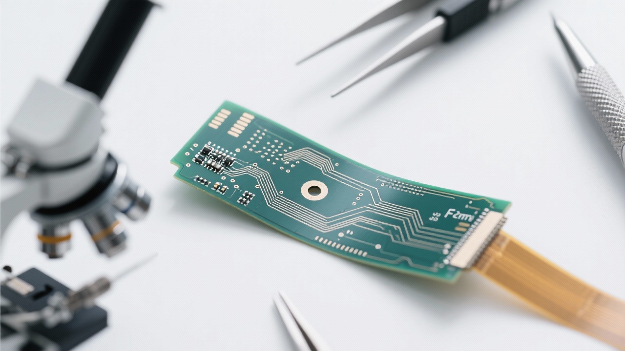
In high-density electronic design, achieving consistent manufacturing at 2mil line width and 0.15mm hole diameter is no longer a theoretical goal—it’s a practical necessity for advanced devices like smartphones, wearables, and aerospace systems. At Ruiheng PCB, we’ve refined our process over 15 years to deliver reliable, repeatable results that meet global standards.

The Foundation: Material Selection & Stack-Up Design

For stable 2mil traces, choosing the right base material is critical. A 0.13mm board thickness with 1oz copper offers optimal balance between flexibility and signal integrity. Our engineers prefer PI (Polyimide) + FR-4 composite materials—not just for mechanical strength, but also for EMI shielding in sensitive environments.

Parameter Recommended Value Why It Matters
Board Thickness 0.13mm Reduces warpage, improves bendability
Copper Weight 1oz (35μm) Balances conductivity and etch precision
Surface Finish ENIG (Electroless Nickel Immersion Gold) Ensures solderability, corrosion resistance, and long-term reliability

Controlled Impedance: Don’t Ignore the Layout

Even with perfect materials, impedance mismatch can ruin signal quality. We recommend controlled impedance routing using tools like Altium or Cadence—ensuring trace width, dielectric constant, and layer spacing are all calculated before fabrication. For 4-layer boards, placing power planes adjacent to signal layers reduces crosstalk by up to 40%.

💡 Design Tip: Always simulate your layout under worst-case conditions—temperature variation, flexing cycles, and moisture exposure—to avoid real-world failures.

0.15mm Holes: Precision Isn’t Just About Drill Size

Drilling holes smaller than 0.2mm requires laser drilling or micro-mechanical drills with tight tolerance control (±0.02mm). At Ruiheng PCB, we use automated optical inspection (AOI) post-drill to verify hole quality and prevent via plugging issues—a common failure point in mass production.

Cross-section of a 4-layer FPC showing stack-up layers including copper thickness, dielectric layers, and via structure.

Our customers report 98% first-pass yield on 0.15mm holes when following our guidelines—especially when combining ENIG surface finish with proper cleaning protocols before assembly.

Common Pitfalls & Real Solutions

Many designers fail because they overlook these three points:

  • Overlooking thermal stress during flexing → Use PI-based substrates with low CTE (Coefficient of Thermal Expansion).
  • Ignoring via-in-pad design rules → Implement staggered via placement to reduce stress concentration.
  • Skipping DFM checks → Run manufacturability reviews early with your PCB partner like Ruiheng PCB.

If you’re designing for medical devices, automotive electronics, or IoT modules, every micron counts—and so does consistency.

Ready to Bring Your High-Density FPC Designs to Life?

With ISO 9001 and IPC-6013-certified processes, Ruiheng PCB delivers rapid prototyping (7-day turnaround) and full-scale production with guaranteed accuracy down to 2mil lines and 0.15mm holes. Let us help you turn complex designs into reliable products—without compromise.

Get Your Free FPC Design Review Today
Name *
Email *
Message*

Recommended Products

Related Reading

How Industrial FPC Achieves 0.05mm Line Width Precision: Optical Imaging and Etching Process Synergy

2026-03-06 | https://shmuker.oss-accelerate.aliyuncs.com/tmp/temporary/60ec5bd7f8d5a86c84ef79f2/60ec5bdcf8d5a86c84ef7a9a/20240305161110/eye.png 101 | https://shmuker.oss-accelerate.aliyuncs.com/tmp/temporary/60ec5bd7f8d5a86c84ef79f2/60ec5bdcf8d5a86c84ef7a9a/20240305160636/lable.png industrial FPC line width precision optical image transfer process precision etching technology ENIG surface finish flexible circuit board manufacturing

0.3mm Microvias and 17:1 Aspect Ratio in 34-Layer HDI PCBs: Signal Integrity for Semiconductor Test Boards

2026-02-11 | https://shmuker.oss-accelerate.aliyuncs.com/tmp/temporary/60ec5bd7f8d5a86c84ef79f2/60ec5bdcf8d5a86c84ef7a9a/20240305161110/eye.png 286 | https://shmuker.oss-accelerate.aliyuncs.com/tmp/temporary/60ec5bd7f8d5a86c84ef79f2/60ec5bdcf8d5a86c84ef7a9a/20240305160636/lable.png 0.3mm microvia HDI PCB 17:1 aspect ratio vias semiconductor test board PCB laser drilling and backdrill control high-speed signal integrity PCB

High-Tg FR-4 4-Layer Thick Copper PCB for Power Electronics: Thermal Performance Explained

2026-03-03 | https://shmuker.oss-accelerate.aliyuncs.com/tmp/temporary/60ec5bd7f8d5a86c84ef79f2/60ec5bdcf8d5a86c84ef7a9a/20240305161110/eye.png 300 | https://shmuker.oss-accelerate.aliyuncs.com/tmp/temporary/60ec5bd7f8d5a86c84ef79f2/60ec5bdcf8d5a86c84ef7a9a/20240305160636/lable.png high-tg fr-4 pcb thick copper pcb power electronics pcb enig surface finish impedance controlled pcb

ENIG Surface Finish Technology Explained: Enhancing Solder Reliability in High-Density Flexible PCBs

2026-03-16 | https://shmuker.oss-accelerate.aliyuncs.com/tmp/temporary/60ec5bd7f8d5a86c84ef79f2/60ec5bdcf8d5a86c84ef7a9a/20240305161110/eye.png 409 | https://shmuker.oss-accelerate.aliyuncs.com/tmp/temporary/60ec5bd7f8d5a86c84ef79f2/60ec5bdcf8d5a86c84ef7a9a/20240305160636/lable.png ENIG surface finish flexible PCB high-density FPC solder reliability impedance control

Why IPC Class 2 PCB Warpage Must Stay Below 0.5% for High-End 34-Layer HDI Boards in Semiconductor Test

2026-02-18 | https://shmuker.oss-accelerate.aliyuncs.com/tmp/temporary/60ec5bd7f8d5a86c84ef79f2/60ec5bdcf8d5a86c84ef7a9a/20240305161110/eye.png 211 | https://shmuker.oss-accelerate.aliyuncs.com/tmp/temporary/60ec5bd7f8d5a86c84ef79f2/60ec5bdcf8d5a86c84ef7a9a/20240305160636/lable.png IPC Class 2 PCB warpage 0.5% warpage HDI PCB 34-layer HDI PCB manufacturing semiconductor test PCB reliability HDI stack-up copper balance
Popular articles
https://shmuker.oss-accelerate.aliyuncs.com/data/oss/20251230/d47ffe47fe3f2d0fde94b14a5ca4b52e/aa681be2-e9be-4c8a-a019-f33ba92e2899.jpeg
https://shmuker.oss-accelerate.aliyuncs.com/data/oss/20251230/141e3615b7cc68db7aeef60572ce0a5a/df049d1d-21f7-4162-8696-74640563c4d1.jpeg
https://shmuker.oss-accelerate.aliyuncs.com/data/oss/20251230/f546ee23d1f5b79cb30ea144c64bf7a0/41080766-f5fe-4275-980d-2f6b2674b30f.jpeg
https://shmuker.oss-accelerate.aliyuncs.com/data/oss/20251230/98a0f8dc62454bf192d2e2ad4121882b/ff001750-26c3-460f-87b7-936299e6380d.jpeg
https://shmuker.oss-accelerate.aliyuncs.com/data/oss/20251230/74cae3ecdb9a0b7f18e44f6631cea9fa/a50611de-8ff5-4f46-a7e1-6a2a52b90b99.jpeg
https://shmuker.oss-accelerate.aliyuncs.com/data/oss/20251230/8b8b1d37b71e344d6a5f246185ce2506/34fa0194-4837-4f46-a9a0-4f56a966047d.jpeg
https://shmuker.oss-accelerate.aliyuncs.com/data/oss/20251230/f546ee23d1f5b79cb30ea144c64bf7a0/41080766-f5fe-4275-980d-2f6b2674b30f.jpeg
https://shmuker.oss-accelerate.aliyuncs.com/data/oss/20251230/e50dd1246854589670af5efeee5d8e1e/68a087cc-9da3-448b-a682-59f50b15a26d.jpeg
Recommended Reading
Contact us
Contact us
https://shmuker.oss-accelerate.aliyuncs.com/tmp/temporary/60ec5bd7f8d5a86c84ef79f2/60ec5bdcf8d5a86c84ef7a9a/thumb-prev.png