
In the realm of 5G and high-frequency communication systems, impedance control remains the linchpin to preserving signal integrity across multilayer printed circuit boards (PCBs). Industry standards settle on 50 Ω single-ended and 100 Ω differential impedance values, driven by the need for optimized signal transmission velocity and minimal reflection. These reference impedances directly influence parameters like insertion loss and crosstalk, critical for sustaining high data rates without degradation.
The 50 Ω single-ended impedance represents an ideal balance between power handling and low attenuation, commonly used for RF circuits and signal lines. Meanwhile, 100 Ω differential impedance supports differential pair signaling, which enhances noise immunity and reduces electromagnetic interference (EMI) by utilizing complementary signals. Such controlled impedance values are pivotal in high-speed digital designs, where even minor deviations can lead to signal reflections and timing errors.
Consider the application of impedance control within a 5G base station’s RF module. The design strategy involves forming precise transmission lines via controlled trace widths, layer stack-ups, and dielectric selections to meet the 50 Ω and 100 Ω targets. Common pitfalls, such as inadequate copper etching tolerances or inconsistent dielectric thickness, often cause impedance drift that results in increased bit error rates (BER).
Practically, line widths as tight as 3 mils (0.0762 mm) are often deployed, paired with solder mask-defined finish layers to curb impedance variation and maintain repeatability at scale. Additional techniques include filling vias under solder masks to prevent impedance discontinuities and signal reflections.
Interactive Question: Have you experienced impedance drift issues in your high-speed PCB projects? What mitigation strategies yielded tangible improvements?
Material selection critically impacts impedance stability. High-performance dielectrics like ISOLA 370HR and MENTRON6 provide stable dielectric constants (Dk ~3.7 to 4.0) and significantly lower dissipation factors (Df < 0.005), minimizing signal loss at gigahertz frequencies. These substrates, paired with copper foil thickness typically ranging from 18 μm to 35 μm, allow for tight line geometry control.
Moreover, multilayer stack designs strategically distribute ground and power planes to yield controlled impedance channel layouts while suppressing electromagnetic interference. Layer lamination pressure, resin flow, and curing cycles are meticulously monitored to avoid variation that could alter dielectric thickness and, by extension, impedance.
To close the loop on manufacturing integrity, engineers leverage sophisticated simulation tools—like finite element method (FEM) and time-domain reflectometry (TDR) models—to predict impedance profiles before fabrication. These simulations integrate precise material parameters and dimensional tolerances to forecast impedance within ±5% of target values.
Post-fabrication, Automated Optical Inspection (AOI) systems scrutinize copper line widths, solder mask coverage, and via fillings to ensure conformance to design specifications. This rigorous inspection correlates strongly with consistent yield rates and minimal rework costs.
 247
|
247
|
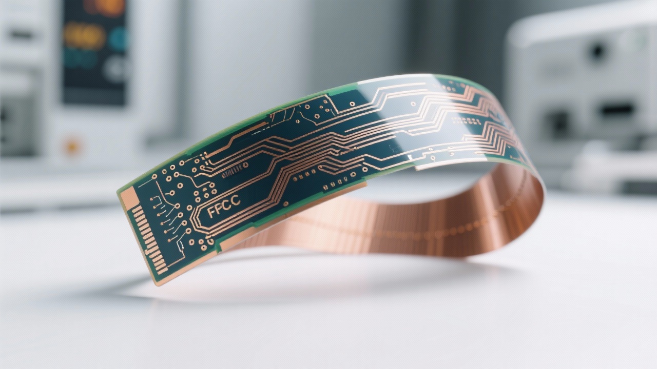
 FPC high-density routing
flexible circuit board design
trace spacing control
EMI shielding in FPC
flexible PCB manufacturing
125
|
high-density FPC layout
flexible PCB design techniques
electromagnetic compatibility optimization
signal crosstalk prevention
advanced flexible PCB manufacturing
459
|
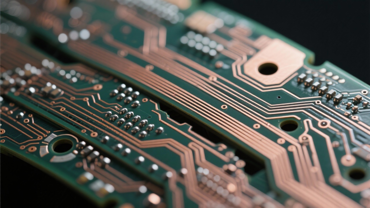
Multilayer FPC Via Design
FPC Bend Area Stress
Flexible Circuit Design
High-Density FPC Routing
FPC Reliability Enhancement
256
|
multilayer flexible pcb via design
high-density fpc routing
fpc electromagnetic compatibility
flexible circuit board manufacturing capability
fpc bend zone reliability
325
|
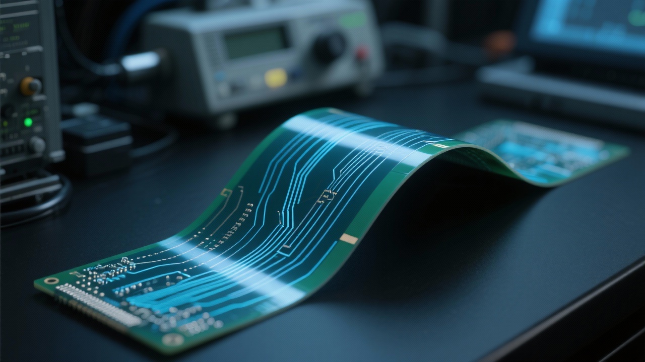
FPC high - density wiring
Flexible circuit board design skills
Via design challenges
Electromagnetic compatibility optimization
Flexible PCB manufacturing process
FPC high-density routing
flexible circuit board design
trace spacing control
EMI shielding in FPC
flexible PCB manufacturing
125
|
high-density FPC layout
flexible PCB design techniques
electromagnetic compatibility optimization
signal crosstalk prevention
advanced flexible PCB manufacturing
459
|
Multilayer FPC Via Design
FPC Bend Area Stress
Flexible Circuit Design
High-Density FPC Routing
FPC Reliability Enhancement
256
|
multilayer flexible pcb via design
high-density fpc routing
fpc electromagnetic compatibility
flexible circuit board manufacturing capability
fpc bend zone reliability
325
|
FPC high - density wiring
Flexible circuit board design skills
Via design challenges
Electromagnetic compatibility optimization
Flexible PCB manufacturing process
-4.png?x-oss-process=image/resize,h_800,m_lfit/format,webp)


-L4-4.png?x-oss-process=image/resize,m_fill,h_800,w_800/format,webp)
-4.png?x-oss-process=image/resize,m_fill,h_800,w_800/format,webp)


