
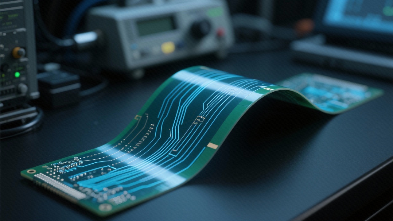
In the era of 5G and high-frequency communication systems, impedance control is no longer optional—it's a non-negotiable requirement for signal integrity. Whether you're designing baseband modules or RF front-ends, understanding how to consistently achieve 50Ω single-ended and 100Ω differential impedance across complex multi-layer boards can make or break your product’s performance.
The choice of 50Ω for single-ended signals and 100Ω for differential pairs isn’t arbitrary—it’s rooted in physics and decades of empirical testing. According to IEEE 2145-2022, these values offer optimal balance between power transfer efficiency and minimal signal loss in coaxial and stripline structures. In real-world applications like mmWave antenna arrays or FPGA interconnects, even a ±5% deviation from target impedance can cause reflections, jitter, and bit error rates (BER) exceeding telecom-grade thresholds (e.g., BER > 1e-12).
High-speed PCBs demand more than just good layout—they need materials with stable Dk (dielectric constant) and low loss tangent. For example, ISOLA 370HR offers a consistent Dk of 3.6 at 1 GHz and a loss tangent below 0.002, making it ideal for 5G mid-band applications. When paired with precise copper thickness control (typically 1 oz/ft² ±5%) and optimized layer stackup—such as inner layers sandwiched between ground planes—you can reduce impedance variation across batches to under 3%. This level of consistency ensures that every board meets telecom reliability standards (e.g., Telcordia GR-468).
Even with perfect design, manufacturing tolerances dictate real-world performance. Key parameters include:

Before production, use tools like SIwave or HyperLynx to simulate impedance profiles under varying conditions. Then, validate with actual measurements using Time Domain Reflectometry (TDR)—a method proven to detect impedance mismatches down to ±2%. Finally, integrate AOI (Automated Optical Inspection) into your process flow to catch defects like incomplete via filling or solder mask bridging that could degrade performance over time.
Real-world case study: A client in Germany achieved ±3.2% impedance accuracy on a 24-layer PCB used in 5G small cells by combining ISOLA 370HR material, tight manufacturing controls, and post-fabrication TDR verification. Their system passed all EMC and signal integrity tests required for EU telecom certification.
We specialize in delivering telecom-grade PCB solutions tailored for 5G infrastructure, radar systems, and AI edge computing platforms. Our team has helped clients reduce impedance-related failures by over 60% through data-driven design and strict quality gates.
Explore our 24-Layer High-Frequency PCB Solutions 419
|
419
|
 FPC high-density routing
flexible PCB design techniques
EMI optimization
signal crosstalk mitigation
flexible PCB manufacturing process
291
|
high-speed multilayer PCB
impedance control
5G communication module
high-frequency PCB design
signal integrity
459
|
Multilayer FPC Via Design
FPC Bend Area Stress
Flexible Circuit Design
High-Density FPC Routing
FPC Reliability Enhancement
317
|
high-density FPC routing
flexible PCB design
EMI optimization
medical FPC
consumer electronics FPC
447
|
FPC high - density wiring
Flexible circuit board design skills
Electromagnetic compatibility optimization
High - density flexible PCB
Via design standards
FPC high-density routing
flexible PCB design techniques
EMI optimization
signal crosstalk mitigation
flexible PCB manufacturing process
291
|
high-speed multilayer PCB
impedance control
5G communication module
high-frequency PCB design
signal integrity
459
|
Multilayer FPC Via Design
FPC Bend Area Stress
Flexible Circuit Design
High-Density FPC Routing
FPC Reliability Enhancement
317
|
high-density FPC routing
flexible PCB design
EMI optimization
medical FPC
consumer electronics FPC
447
|
FPC high - density wiring
Flexible circuit board design skills
Electromagnetic compatibility optimization
High - density flexible PCB
Via design standards

-1.png?x-oss-process=image/resize,h_800,m_lfit/format,webp)


-1.png?x-oss-process=image/resize,m_fill,h_800,w_800/format,webp)
-4.png?x-oss-process=image/resize,m_fill,h_800,w_800/format,webp)

-L4-4.png?x-oss-process=image/resize,m_fill,h_800,w_800/format,webp)
