
In high - speed signal transmission, impedance matching is of utmost importance. When the impedance of the signal source, transmission line, and load are not matched, it can lead to signal reflection and distortion. For example, in a high - speed PCB with a clock frequency of 1GHz, a mismatch in impedance can cause up to 30% of the signal energy to be reflected back, which significantly degrades the signal quality. The industry has reached a consensus on the 50 - ohm single - ended and 100 - ohm differential impedance standards. These standards are widely used in various high - speed communication systems, providing a unified design reference for engineers.
Single - ended impedance refers to the impedance between a single signal line and the reference ground. In high - speed PCB design, a common single - ended impedance value is 50 ohms. Differential impedance, on the other hand, is the impedance between two complementary signal lines in a differential pair. The standard differential impedance is 100 ohms.
Single - ended impedance is often used in general - purpose signal transmission, such as power supply lines and some low - speed control signals. Differential impedance is mainly used in high - speed data transmission interfaces, like USB 3.0, HDMI, and Ethernet. These interfaces require high - speed and reliable data transfer, and differential signaling can effectively reduce electromagnetic interference and crosstalk.
Single - ended signals are more susceptible to external interference and ground noise. Any change in the impedance of the single - ended line can cause signal reflection. Differential signals, due to their complementary nature, can cancel out common - mode noise. However, if the impedance of the two lines in a differential pair is not well - matched, it can also lead to differential - mode noise and affect signal integrity.
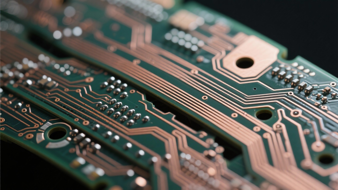
Several parameters have a significant impact on impedance stability. The dielectric constant of the medium affects the propagation speed of the signal in the PCB. For example, a medium with a high dielectric constant will slow down the signal propagation. Copper foil thickness also matters. A thicker copper foil can reduce the resistance of the signal line but may also affect the impedance value. The layer - stack structure is another crucial factor. A well - designed layer - stack can ensure uniform impedance distribution. For instance, a four - layer PCB with a proper arrangement of power, ground, and signal layers can better control impedance. A typical line width in high - speed PCB design might be 3mil, and using solder mask to protect vias can also help maintain impedance stability.
Taking the PCB of a 5G base station as an example, during the design phase, engineers need to predict and optimize impedance values. They need to consider the high - frequency characteristics of the 5G signals, such as the high - frequency range from 24GHz to 52GHz. By using high - performance dielectric materials like ISOLA 370HR and Panasonic MENTRON6, and carefully designing the layer - stack structure, engineers can achieve stable impedance control. In the 5G base station PCB design, accurate impedance control can reduce signal loss by up to 20% and improve the overall performance of the base station.
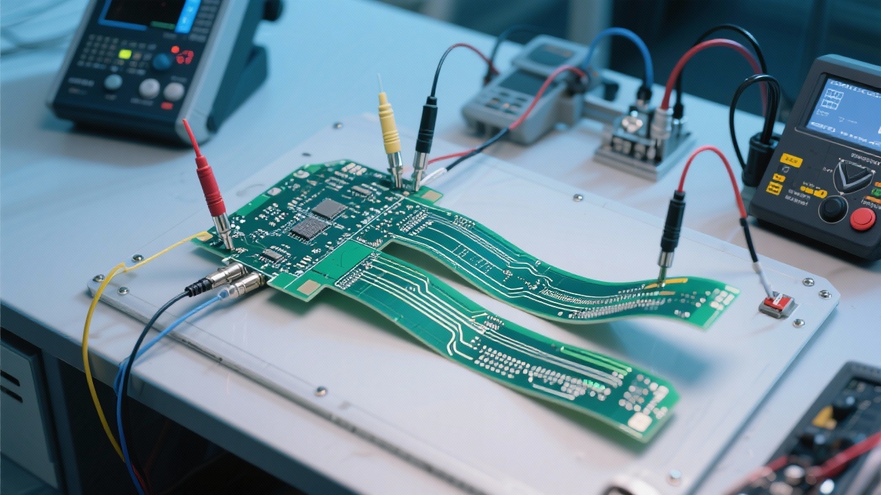
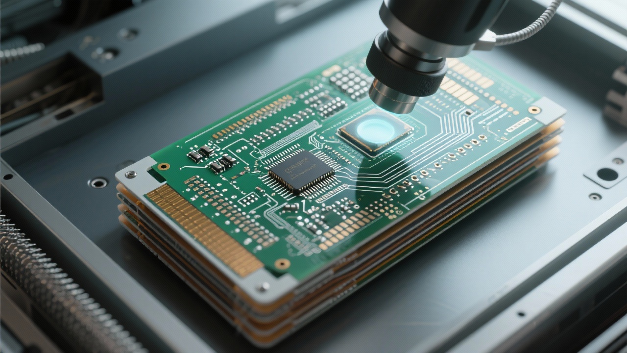
Impedance simulation tools such as HFSS and SIwave are widely used in the design phase. These tools can simulate the impedance characteristics of the PCB under different conditions, helping engineers to optimize the design. AOI (Automated Optical Inspection) is used in mass production. It can quickly and accurately detect defects on the PCB, such as short - circuits and open - circuits, which may affect impedance. By combining these two methods, engineers can ensure the impedance accuracy of the PCB in mass production.
Quality control throughout the process from design to manufacturing to testing is crucial. A well - established quality control loop can improve customer trust. By strictly controlling every step, from selecting high - quality materials to using advanced manufacturing and testing techniques, the reliability of the PCB can be guaranteed. This is especially important for next - generation telecommunication equipment, which requires high - performance and stable PCBs.
Welcome to consult our high - reliability PCB solutions specially designed for high - frequency telecommunication projects. Click here to learn more
 98
|
98
|
 high-speed multilayer PCB
impedance control
high-performance dielectric materials
5G base stations
signal integrity
114
|
High-speed multilayer PCB
Impedance control
5G base station
High-frequency communication module
AOI detection
430
|
high-speed multilayer pcb impedance control
50 ohm single ended impedance
100 ohm differential impedance
high frequency pcb design
signal integrity optimization
459
|
Multilayer FPC Via Design
FPC Bend Area Stress
Flexible Circuit Design
High-Density FPC Routing
FPC Reliability Enhancement
156
|
multilayer flexible pcb via design
micro-hole processing in fpc
high-density flex pcb layout
emc optimization in flexible circuits
flexible pcb manufacturing process
high-speed multilayer PCB
impedance control
high-performance dielectric materials
5G base stations
signal integrity
114
|
High-speed multilayer PCB
Impedance control
5G base station
High-frequency communication module
AOI detection
430
|
high-speed multilayer pcb impedance control
50 ohm single ended impedance
100 ohm differential impedance
high frequency pcb design
signal integrity optimization
459
|
Multilayer FPC Via Design
FPC Bend Area Stress
Flexible Circuit Design
High-Density FPC Routing
FPC Reliability Enhancement
156
|
multilayer flexible pcb via design
micro-hole processing in fpc
high-density flex pcb layout
emc optimization in flexible circuits
flexible pcb manufacturing process


-1.png?x-oss-process=image/resize,m_fill,h_800,w_800/format,webp)

-L4-4.png?x-oss-process=image/resize,m_fill,h_800,w_800/format,webp)

