
In the era of 5G and high-frequency telecommunication systems, impedance control stands as the cornerstone for ensuring signal integrity. As the demand for high-speed data transmission grows, the importance of impedance control in high-speed printed circuit boards (PCBs) cannot be overstated. It is crucial for maintaining the reliability of next-generation telecommunication systems.
The 50 ohm single-ended and 100 ohm differential impedance standards are widely used in high-speed data transmission. The 50 ohm single-ended impedance is designed to minimize power loss and signal reflection, which is suitable for most high-speed single-ended signal transmission scenarios. The 100 ohm differential impedance, on the other hand, is used for differential signal transmission, which can effectively reduce electromagnetic interference and improve signal quality. These two impedance standards are the key to achieving high-speed and reliable data transmission in high-frequency PCBs.
High-performance dielectric materials play a vital role in impedance stability. Materials like ISOLA 370HR and MENTRON6 have excellent electrical properties, such as low dielectric constant and low loss tangent, which can effectively reduce signal attenuation and improve impedance stability. The choice of appropriate dielectric materials is essential for achieving stable impedance performance in high-frequency PCBs.
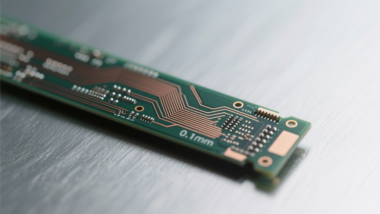
To achieve the desired impedance performance, the manufacturing process must be carefully controlled. Factors such as copper thickness, lamination tolerance, and ENIG surface treatment can all affect the impedance of the PCB. For example, a copper thickness of 1oz can provide better conductivity, while a tight lamination tolerance of ±1mil can ensure the accuracy of the PCB's layer structure. The ENIG surface treatment can improve the solderability and corrosion resistance of the PCB, which is beneficial for maintaining the long-term stability of the impedance.
Let's take a look at a practical engineering case: the impedance matching strategy in 5G RF modules. In this case, a 5G base station module was designed with a focus on impedance control. By using high-performance dielectric materials and precise manufacturing processes, a stable impedance performance was achieved. The design used a 3mil line width/space and a tight manufacturing tolerance to ensure the accuracy of the impedance. The AOI (Automated Optical Inspection) was also used to detect any potential defects in the PCB, which helped to improve the reliability of the product.
AOI testing and simulation tools are essential for quality control in high-frequency PCB manufacturing. AOI testing can detect any physical defects in the PCB, such as open circuits, short circuits, and incorrect line widths. Simulation tools can be used to predict the impedance performance of the PCB before manufacturing, which can help to optimize the design and reduce the risk of failure. By using these tools, manufacturers can ensure the quality and reliability of their high-frequency PCBs.
Our 24-layer high-frequency PCBs have successfully served leading global telecommunication enterprises. With precise impedance control and strict AOI testing, we can help you build more reliable and high-performance next-generation communication devices. Don't miss this opportunity to enhance the reliability of your projects. Click here to learn how we can empower your projects!
 358
|
358
|
 高密度柔性PCB设计
柔性电路板布局优化
FPC中的电磁兼容性
细间距PCB制造
消费电子产品柔性PCB
247
|
FPC高密度布线
柔性电路板设计
迹线间距控制
FPC中的EMI屏蔽
柔性PCB制造
220
|
FPC高密度布线
柔性电路板设计技术
电磁兼容性优化
高密度布线解决方案
柔性PCB制造工艺
325
|
FPC高密度布线
柔性电路板设计技能
通过设计挑战
电磁兼容性优化
柔性PCB制造工艺
447
|
FPC高密度布线
柔性电路板设计技能
电磁兼容性优化
高密度柔性PCB
通过设计标准
高密度柔性PCB设计
柔性电路板布局优化
FPC中的电磁兼容性
细间距PCB制造
消费电子产品柔性PCB
247
|
FPC高密度布线
柔性电路板设计
迹线间距控制
FPC中的EMI屏蔽
柔性PCB制造
220
|
FPC高密度布线
柔性电路板设计技术
电磁兼容性优化
高密度布线解决方案
柔性PCB制造工艺
325
|
FPC高密度布线
柔性电路板设计技能
通过设计挑战
电磁兼容性优化
柔性PCB制造工艺
447
|
FPC高密度布线
柔性电路板设计技能
电磁兼容性优化
高密度柔性PCB
通过设计标准
-1.png?x-oss-process=image/resize,h_800,m_lfit/format,webp)


-L4-4.png?x-oss-process=image/resize,m_fill,h_800,w_800/format,webp)
-1.png?x-oss-process=image/resize,m_fill,h_800,w_800/format,webp)

-4.png?x-oss-process=image/resize,m_fill,h_800,w_800/format,webp)

