
As the demand for faster and more reliable telecommunications infrastructure surges, especially with the rollout of 5G base stations and advanced high-frequency communication modules, ensuring signal integrity on printed circuit boards (PCBs) becomes paramount. Central to this challenge is the control of impedance in high-speed multilayer PCBs, where even minor deviations can cause significant signal degradation. This article explores the critical role that high-performance dielectric materials play in stabilizing impedance, reducing signal reflection, and minimizing crosstalk in high-frequency environments.
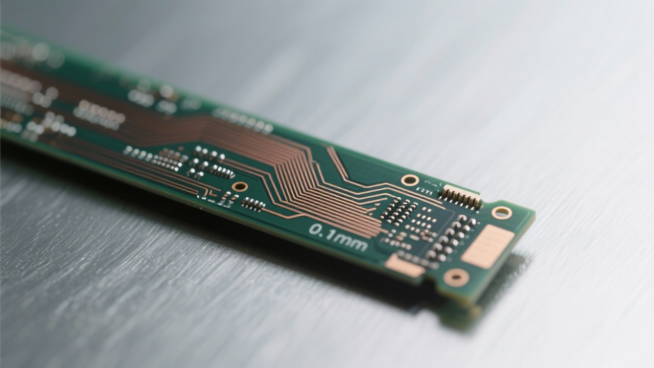
Controlled impedance is the cornerstone of signal integrity in high-speed PCBs. The industry commonly adopts two impedance standards: 50 ohms for single-ended signals and 100 ohms for differential pairs. These standards ensure minimal signal reflection and optimal timing margins at GHz frequencies. In practice, achieving these impedance values requires precise moderation of dielectric constants (Dk), conductor geometry, and stackup configurations.
The impedance (Z) of a transmission line on a PCB is governed by the relationship:
Z = (87 / √(ε_r + 1.41)) * ln(5.98 * h / (0.8 * w + t))
where ε_r is the dielectric constant, h is the dielectric thickness, w is the trace width, and t is the trace thickness. Even minor fluctuations in the dielectric constant or physical dimensions can shift impedance out of specification.
5G networks operate at increasingly higher frequency bands (sub-6 GHz and millimeter-wave bands), where signal integrity challenges intensify. For example, differential pairs in radio-frequency front-end modules demand strict impedance matching to maintain data throughput and reduce bit error rates below 10-12.
In a case study involving a 5G base station PCB, slight deviations of ±5% in dielectric constant led to more than 15% impedance mismatch, causing signal reflections and degraded signal-to-noise ratio (SNR). This emphasizes the necessity of ultra-stable materials and precise manufacturing processes.
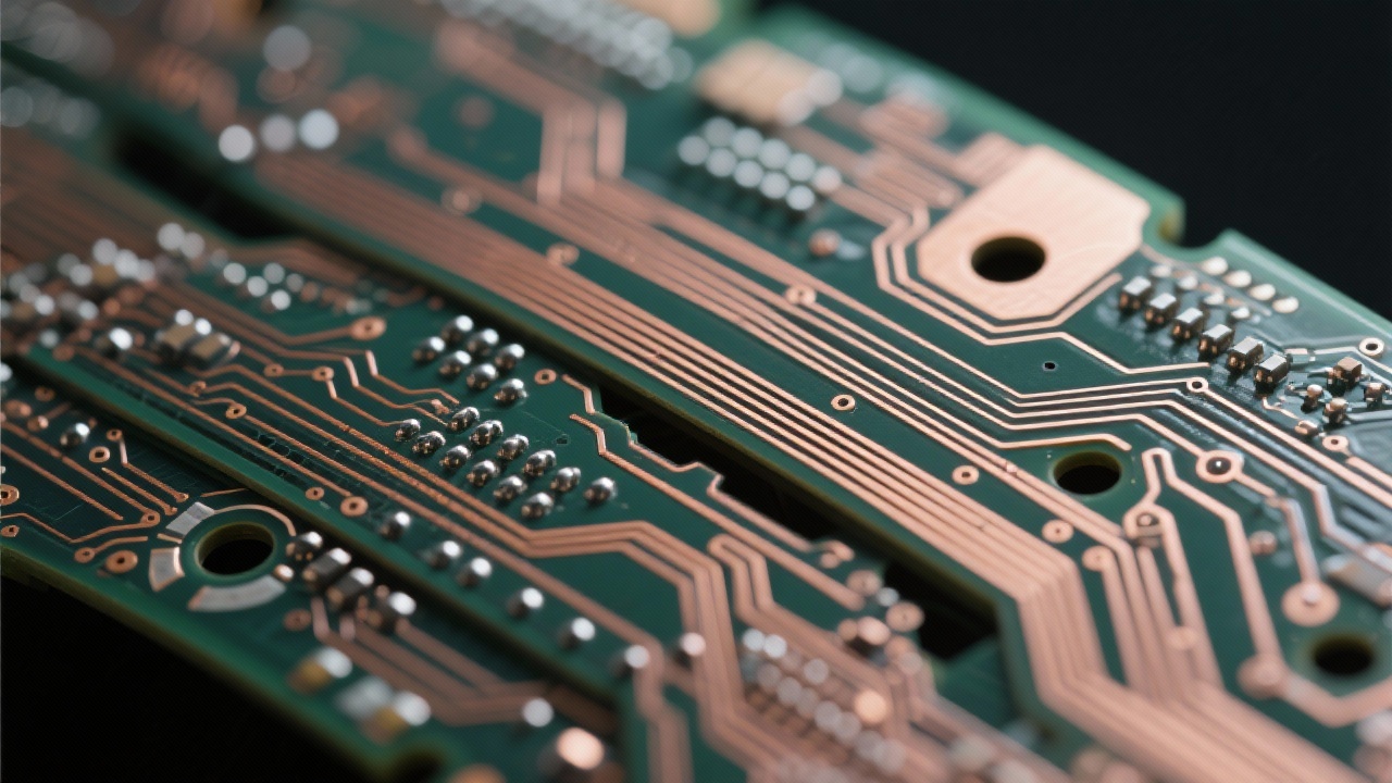
High-performance dielectric substrates such as low-loss Rogers materials, advanced FR-4 variants with tightly controlled Dk and dissipation factor (Df), are instrumental in achieving impedance stability. These materials boast dielectric constants as low as 3.3 and Df values below 0.0017, significantly less than standard FR-4.
Moreover, precision lamination processes allow for consistent dielectric thickness tolerances as tight as ±2 microns, mitigating manufacturing-induced impedance variations. Multilayer PCBs configured with symmetrical stackups and controlled trace geometries reduce crosstalk and electromagnetic interference (EMI), further preserving signal fidelity.
Verifying impedance compliance through both simulation and physical measurement is critical in high-speed PCB manufacturing. Electromagnetic field simulators provide accurate design validation by predicting impedance and coupling effects before fabrication. After production, Time Domain Reflectometry (TDR) measurements empirically confirm impedance values along critical signal traces.
Automated Optical Inspection (AOI) further enhances quality control by detecting micro-scale defects, layer misalignment, and trace width variations that can impact impedance performance. Integrating these technologies into the manufacturing workflow reduces scrap rates by up to 30% and ensures yield consistency.
Are you ready to elevate your high-frequency PCB designs with cutting-edge materials and precision manufacturing?
Explore Our High-Performance PCB Manufacturing Solutions 419
|
419
|
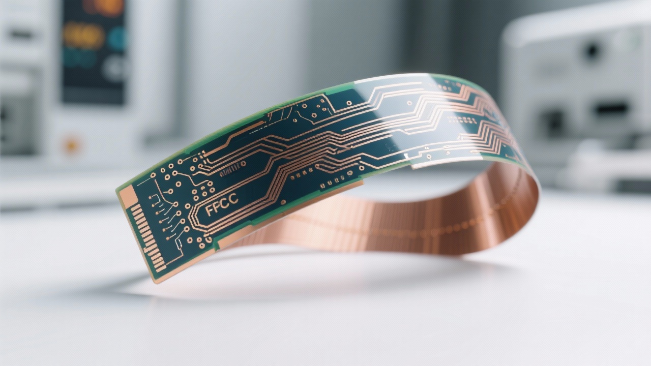
 Flexible Leiterplatte Design
Signalinterferenz vermeiden
EMV Optimierung FPC
Hochdichte FPC-Bestückung
FPC Herstellungstechnologie
402
|
FPC Hochdichte-Leiterbahnen
flexible Schaltungstechnik
Leiterbahnabstand 0
1 mm
elektromagnetische Verträglichkeit
flexible Leiterplattenfertigung
459
|
FPC Via Design
FPC Biegebereich Spannungskonzentration
Flexibles Leiterplatten Design
Hochdichtverdrahtung
Signalintegrität FPC
256
|
multilayer flexible pcb via design
high-density fpc routing
fpc electromagnetic compatibility
flexible circuit board design
precision via fabrication
298
|
Hochdichte Verdrahtung von FPCs
Designtechniken für flexible Leiterplatten
Optimierung der elektromagnetischen Verträglichkeit
Schutz gegen Signalkreuzstörungen
Herstellung von FPCs mit hoher Zuverlässigkeit
Flexible Leiterplatte Design
Signalinterferenz vermeiden
EMV Optimierung FPC
Hochdichte FPC-Bestückung
FPC Herstellungstechnologie
402
|
FPC Hochdichte-Leiterbahnen
flexible Schaltungstechnik
Leiterbahnabstand 0
1 mm
elektromagnetische Verträglichkeit
flexible Leiterplattenfertigung
459
|
FPC Via Design
FPC Biegebereich Spannungskonzentration
Flexibles Leiterplatten Design
Hochdichtverdrahtung
Signalintegrität FPC
256
|
multilayer flexible pcb via design
high-density fpc routing
fpc electromagnetic compatibility
flexible circuit board design
precision via fabrication
298
|
Hochdichte Verdrahtung von FPCs
Designtechniken für flexible Leiterplatten
Optimierung der elektromagnetischen Verträglichkeit
Schutz gegen Signalkreuzstörungen
Herstellung von FPCs mit hoher Zuverlässigkeit
-4.png?x-oss-process=image/resize,h_800,m_lfit/format,webp)


-L4-4.png?x-oss-process=image/resize,m_fill,h_800,w_800/format,webp)

-1.png?x-oss-process=image/resize,m_fill,h_800,w_800/format,webp)


