Achieving 0.05mm Line Width and Spacing in Industrial FPC: Precision Manufacturing Techniques Explained

Ruiheng PCB
2026-03-08
Technical knowledge
Struggling with signal integrity or functional failures due to FPC line width deviations? This article dives into how Ruiheng PCB delivers industrial-grade flexible circuit boards with 0.05mm minimum line width and spacing—detailing optical image transfer, precise etching control, and ENIG surface finish benefits. Real-world case studies show how integrated DIP+SMT assembly capabilities reduce debugging time and rework costs, accelerating high-density electronics to mass production.
https://shmuker.oss-accelerate.aliyuncs.com/data/oss/20251230/10162eed1c55dc9d2c2f47a0acfd4f76/514a91c4-e6c4-488d-a6e8-0a112d4b66b7.jpeg

How to Achieve 0.05mm Line Width and Spacing in Industrial-Grade FPCs

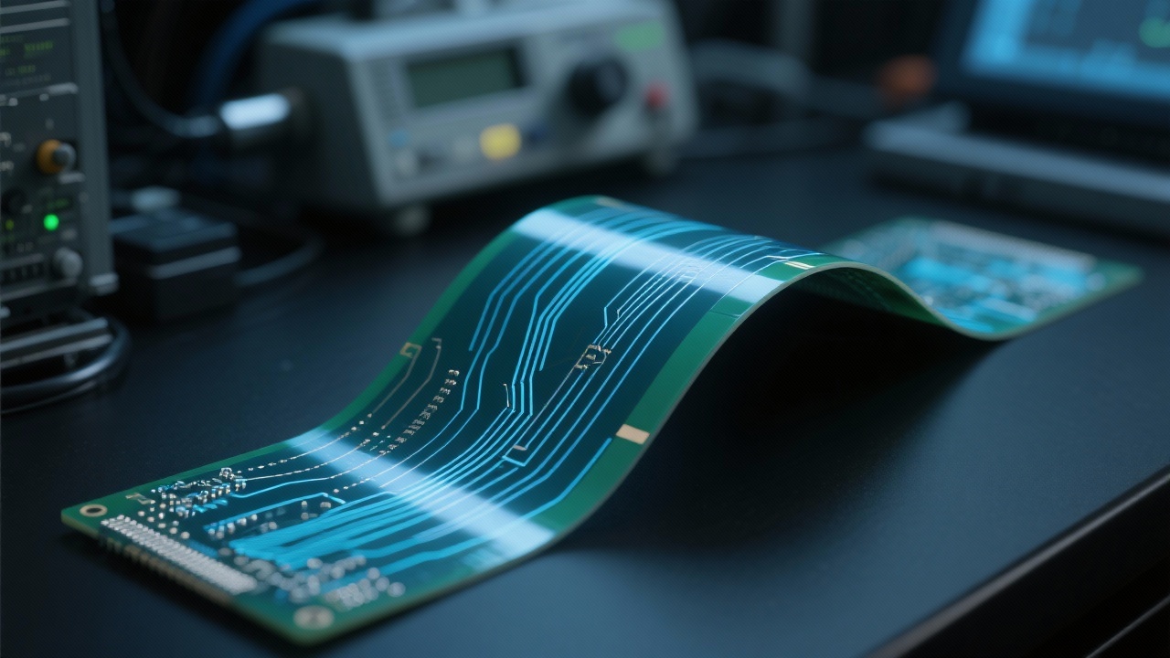
In high-density electronics like medical devices, automotive sensors, and 5G modules, even minor deviations in flexible printed circuit (FPC) line width can cause signal crosstalk or complete functional failure. For engineers pushing the limits of miniaturization, achieving consistent 0.05mm minimum line width and spacing isn't just a goal—it's a requirement.

Precision Starts with Optical Image Transfer

The foundation of micro-scale FPC fabrication lies in optical image transfer—a process where photomasks are projected onto copper-clad laminates using UV exposure systems. According to IPC-2221 standards, a typical industrial-grade setup achieves ±5μm tolerance at 0.05mm features. This precision is critical when designing for frequencies above 6 GHz, where impedance control becomes paramount.

Optical image transfer process showing UV exposure on copper-clad laminate for fine-line FPC manufacturing

Controlled Etching: The Key to Consistency

Once the pattern is transferred, precise chemical etching ensures minimal undercutting. At Ruiheng PCB, our proprietary multi-stage etch bath system maintains uniformity across entire panels—reducing variation from ±10% to under ±3%. This level of control directly impacts yield rates: one client reported a 17% reduction in rework after switching to our process flow.

Pro Tip: When specifying FPC designs, always include a 0.1mm clearance between adjacent traces—even if your design allows tighter spacing—to account for real-world manufacturing variance.

Surface Finish Matters: Why ENIG Wins for High-Density Applications

For applications requiring repeated flexing—such as foldable smartphones or wearable tech—the choice of surface finish significantly affects long-term reliability. While immersion tin may offer lower cost, ENIG (Electroless Nickel Immersion Gold) provides superior solderability, corrosion resistance, and mechanical durability. Industry data shows ENIG-treated boards maintain >95% bond strength after 50,000 bend cycles—far exceeding alternatives.

Comparison chart of different surface finishes: ENIG vs. Immersion Tin vs. HASL – highlighting bending life and solderability performance

One Stop Shop = Faster Time-to-Market

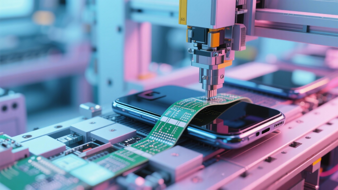
Many companies still separate FPC fabrication from DIP+SMT assembly, leading to delays during prototyping. With integrated capabilities—from layout review to full test verification—Ruiheng PCB reduces debugging time by up to 40%. One customer in the IoT sector cut their first production run from 12 weeks to 7 simply by working with a single supplier who understands both design intent and manufacturability.

“We used to lose 3–5 days per iteration just coordinating between vendors. Now we get feedback within 24 hours.” — Senior Design Engineer, MedTech Startup

Design Rules That Work: Practical Takeaways

  • Use 4-layer stack-ups for better thermal management in dense layouts
  • Apply edge protection (e.g., conformal coating or adhesive tape) near stress points
  • Specify trace width tolerances explicitly—don’t assume they’ll be handled automatically
  • Include test points for electrical verification early in the design phase

Ready to explore how Ruiheng PCB’s precision engineering can support your next-generation FPC project?

Download Our Industrial FPC Design Guide
Name *
Email *
Message*

Recommended Products

Related Reading

Enhancing Consumer Electronics Performance with High-Density Flexible PCB Design

2026-01-03 | https://shmuker.oss-accelerate.aliyuncs.com/tmp/temporary/60ec5bd7f8d5a86c84ef79f2/60ec5bdcf8d5a86c84ef7a9a/20240305161110/eye.png 358 | https://shmuker.oss-accelerate.aliyuncs.com/tmp/temporary/60ec5bd7f8d5a86c84ef79f2/60ec5bdcf8d5a86c84ef7a9a/20240305160636/lable.png high-density flexible PCB design flexible circuit board layout optimization electromagnetic compatibility in FPC fine pitch PCB manufacturing consumer electronics flexible PCB

Enhance Flexible PCB Design Efficiency: High-Density Routing Solutions with Latest Manufacturing Processes

2026-01-14 | https://shmuker.oss-accelerate.aliyuncs.com/tmp/temporary/60ec5bd7f8d5a86c84ef79f2/60ec5bdcf8d5a86c84ef7a9a/20240305161110/eye.png 220 | https://shmuker.oss-accelerate.aliyuncs.com/tmp/temporary/60ec5bd7f8d5a86c84ef79f2/60ec5bdcf8d5a86c84ef7a9a/20240305160636/lable.png FPC high - density routing Flexible circuit board design techniques Electromagnetic compatibility optimization High - density routing solutions Flexible PCB manufacturing processes

High-Speed Multilayer PCB Impedance Measurement and AOI Detection Technology Tutorial: Enhance Product Quality and Signal Integrity

2026-01-28 | https://shmuker.oss-accelerate.aliyuncs.com/tmp/temporary/60ec5bd7f8d5a86c84ef79f2/60ec5bdcf8d5a86c84ef7a9a/20240305161110/eye.png 316 | https://shmuker.oss-accelerate.aliyuncs.com/tmp/temporary/60ec5bd7f8d5a86c84ef79f2/60ec5bdcf8d5a86c84ef7a9a/20240305160636/lable.png High-speed multilayer PCB Impedance control technology AOI detection Signal integrity 5G communication PCB

0.1mm Microvias & 0.5mm Backdrilling: Synergistic Control in High-End HDI PCB Manufacturing

2026-02-14 | https://shmuker.oss-accelerate.aliyuncs.com/tmp/temporary/60ec5bd7f8d5a86c84ef79f2/60ec5bdcf8d5a86c84ef7a9a/20240305161110/eye.png 479 | https://shmuker.oss-accelerate.aliyuncs.com/tmp/temporary/60ec5bd7f8d5a86c84ef79f2/60ec5bdcf8d5a86c84ef7a9a/20240305160636/lable.png HDI PCB Manufacturing 0.1mm Microvia Process 0.5mm Backdrilling Technology PCB Microvia Formation IPC-III Standard

Research on Via Design Challenges and Manufacturing Process Support in High-Density Wiring of Multi-Layer Flexible Circuit Boards

2026-01-02 | https://shmuker.oss-accelerate.aliyuncs.com/tmp/temporary/60ec5bd7f8d5a86c84ef79f2/60ec5bdcf8d5a86c84ef7a9a/20240305161110/eye.png 325 | https://shmuker.oss-accelerate.aliyuncs.com/tmp/temporary/60ec5bd7f8d5a86c84ef79f2/60ec5bdcf8d5a86c84ef7a9a/20240305160636/lable.png FPC high - density wiring Flexible circuit board design skills Via design challenges Electromagnetic compatibility optimization Flexible PCB manufacturing process
Popular articles
https://shmuker.oss-accelerate.aliyuncs.com/data/oss/20251230/e27c0d48147daaf89d42615115b5f11b/45f97e58-2cdb-4b1e-8901-1445a87ab7e5.jpeg
https://shmuker.oss-accelerate.aliyuncs.com/data/oss/20251230/141e3615b7cc68db7aeef60572ce0a5a/df049d1d-21f7-4162-8696-74640563c4d1.jpeg
https://shmuker.oss-accelerate.aliyuncs.com/data/oss/20251230/10162eed1c55dc9d2c2f47a0acfd4f76/514a91c4-e6c4-488d-a6e8-0a112d4b66b7.jpeg
https://shmuker.oss-accelerate.aliyuncs.com/data/oss/20251230/76402db4ddda640df1d8ea772a31c807/0ec0487d-c513-4ae1-bddb-49f7de806bce.jpeg
https://shmuker.oss-accelerate.aliyuncs.com/data/oss/20251230/f546ee23d1f5b79cb30ea144c64bf7a0/41080766-f5fe-4275-980d-2f6b2674b30f.jpeg
https://shmuker.oss-accelerate.aliyuncs.com/data/oss/20251230/141e3615b7cc68db7aeef60572ce0a5a/df049d1d-21f7-4162-8696-74640563c4d1.jpeg
https://shmuker.oss-accelerate.aliyuncs.com/data/oss/20251230/f546ee23d1f5b79cb30ea144c64bf7a0/41080766-f5fe-4275-980d-2f6b2674b30f.jpeg
https://shmuker.oss-accelerate.aliyuncs.com/data/oss/20251230/6361a7640bda96ec7b6928195a7b0ab9/0cff8b23-5c1d-4865-9c37-40619b2a114b.jpeg
https://shmuker.oss-accelerate.aliyuncs.com/data/oss/692910f1af15994642dab58b/692a498eaf15994642dace1b/20251216152709/24-layer-circuit-board-4.png
https://shmuker.oss-accelerate.aliyuncs.com/data/oss/20251230/f546ee23d1f5b79cb30ea144c64bf7a0/41080766-f5fe-4275-980d-2f6b2674b30f.jpeg
Recommended Reading
Contact us
Contact us
https://shmuker.oss-accelerate.aliyuncs.com/tmp/temporary/60ec5bd7f8d5a86c84ef79f2/60ec5bdcf8d5a86c84ef7a9a/thumb-prev.png