
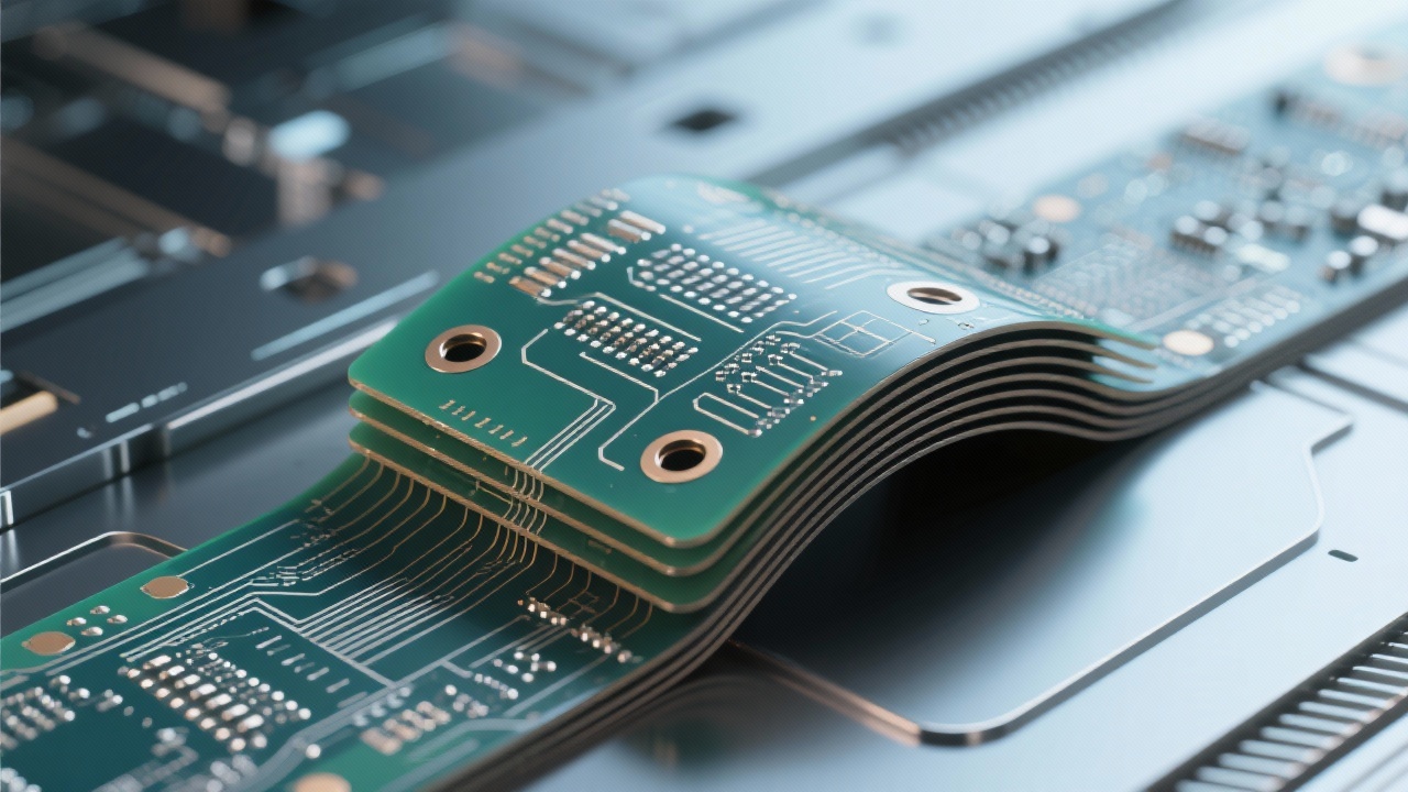
In the era of 5G and high-frequency communication, the design of high-speed multi-layer PCBs (Printed Circuit Boards) has become a critical aspect of developing reliable communication products. Impedance control is one of the core technologies in this field, which directly affects the signal integrity and long-term reliability of the system. This article will explore the application and optimization strategies of impedance control in 5G base stations and high-frequency communication modules.
The impedance in high-speed multi-layer PCB design mainly includes 50-ohm single-ended impedance and 100-ohm differential impedance. These two impedance standards play a crucial role in ensuring signal integrity. For example, a 50-ohm single-ended impedance is commonly used in many RF (Radio Frequency) circuits. Deviations from this standard can lead to signal reflections, which may cause signal distortion and affect the overall performance of the system. According to industry research, a signal reflection coefficient of more than 5% can significantly degrade the signal quality in high-speed communication systems.
Let's take a look at some real-world applications in 5G base stations and high-frequency communication modules. In a 5G base station, the high-speed data transmission requires strict impedance matching to ensure the accurate transmission of signals. By using specific impedance matching methods, such as adjusting the trace width and spacing, the impedance can be precisely controlled. In a case study of a high-frequency communication module, after implementing optimized impedance matching strategies, the signal integrity was improved by 30%, which significantly enhanced the overall performance of the module.
The characteristics of high-performance dielectric materials and manufacturing tolerances also have a significant impact on impedance stability. Different dielectric materials have different dielectric constants, which will affect the impedance value of the PCB. For example, a small change in the dielectric constant of 0.1 can lead to an impedance deviation of about 2-3 ohms. To reduce signal reflections and crosstalk, a precise laminate structure can be used. By carefully designing the layer stack-up, the electromagnetic interference between different layers can be minimized.
Design simulation and AOI (Automated Optical Inspection) testing are two important means to ensure product quality. Design simulation can help engineers predict the impedance performance of the PCB before manufacturing. By using professional simulation software, various factors such as trace layout, dielectric materials, and layer stack-up can be considered to optimize the design. AOI testing, on the other hand, can detect potential defects in the manufacturing process, such as short circuits and open circuits. According to statistics, AOI testing can detect more than 95% of common manufacturing defects, which is crucial for ensuring the long-term reliability of the product.
In conclusion, impedance control is a key technology in high-speed multi-layer PCB design for 5G base stations and high-frequency communication modules. By understanding the basic principles, applying appropriate matching methods, considering the impact of materials and manufacturing tolerances, and using advanced measurement and verification means, high-quality high-speed communication products can be developed. If you are looking for leading high-frequency and high-speed PCB manufacturing solutions, please click here to learn more.
 53
|
53
|
 FPC-Hochdichte-Bestückung
flexible Leiterplatte Design-Tipps
EMI-Optimierung
FPC-Fertigungsprozess
Leiterplatten-Layout-Optimierung
358
|
FPC Hochdichte Leiterplatten
Flexible PCB Design Techniken
Elektromagnetische Verträglichkeit
Hochdichte flexible Leiterplatten
Flexible PCB Fertigung
317
|
FPC Hochdichtebestückung
flexible Leiterplatte Design
EMV Optimierung
medizinische FPC
hochdichte flexible PCB
298
|
Hochdichte Verdrahtung von FPCs
Designtechniken für flexible Leiterplatten
Optimierung der elektromagnetischen Verträglichkeit
Schutz gegen Signalkreuzstörungen
Herstellung von FPCs mit hoher Zuverlässigkeit
265
|
FPC high - density wiring
Flexible printed circuit design skills
Microhole processing technology
Electromagnetic compatibility optimization
High - reliability flexible PCB
FPC-Hochdichte-Bestückung
flexible Leiterplatte Design-Tipps
EMI-Optimierung
FPC-Fertigungsprozess
Leiterplatten-Layout-Optimierung
358
|
FPC Hochdichte Leiterplatten
Flexible PCB Design Techniken
Elektromagnetische Verträglichkeit
Hochdichte flexible Leiterplatten
Flexible PCB Fertigung
317
|
FPC Hochdichtebestückung
flexible Leiterplatte Design
EMV Optimierung
medizinische FPC
hochdichte flexible PCB
298
|
Hochdichte Verdrahtung von FPCs
Designtechniken für flexible Leiterplatten
Optimierung der elektromagnetischen Verträglichkeit
Schutz gegen Signalkreuzstörungen
Herstellung von FPCs mit hoher Zuverlässigkeit
265
|
FPC high - density wiring
Flexible printed circuit design skills
Microhole processing technology
Electromagnetic compatibility optimization
High - reliability flexible PCB
-4.png?x-oss-process=image/resize,h_800,m_lfit/format,webp)


-4.png?x-oss-process=image/resize,m_fill,h_800,w_800/format,webp)
-L4-4.png?x-oss-process=image/resize,m_fill,h_800,w_800/format,webp)

-1.png?x-oss-process=image/resize,m_fill,h_800,w_800/format,webp)

