
The rapid manufacturing of double-sided printed circuit boards (PCBs) involves a series of meticulous processes that balance precision, speed, and quality control. This article delves into the essential steps spanning from initial design input through to flying probe testing, highlighting critical process parameters and technical challenges. Electrical engineers, production managers, and procurement decision-makers can leverage these insights to optimize their product development cycles and supply chain responsiveness.
The manufacturing journey begins with precise design input, where CAD files must meet stringent format and layer specifications. Double-sided PCB designs typically require separate data layers for top and bottom conductive patterns. Utilizing formats such as Gerber X2 enhances data integrity and process automation. Accurate data translation minimizes errors downstream, directly impacting etching accuracy and overall yield.
Integration of design-for-manufacturing (DFM) guidelines also plays a pivotal role. Common challenges include ensuring via placement with respect to copper traces, maintaining adequate clearance between pads, and anticipating layer alignment tolerances within ±25 µm. Early resolution of these factors reduces production reworks and shortens lead times.
Etching precision remains a technical focal point, demanding tight control over acid concentration and exposure time. For example, copper trace widths as narrow as 75 µm require process stability within ±5 µm to maintain circuit integrity. Innovative techniques such as photo-imaging combined with optimized wet-etching yield repeatable results.
Layer lamination incorporates controlled temperature and pressure cycles to ensure strong adhesion between substrate layers and copper foils. Common practice involves lamination at temperatures between 180–200°C under pressures of 2–4 MPa for approximately 60 minutes. Proper lamination prevents micro-delamination and enhances mechanical resilience.
Precision drilling establishes vias critical for interlayer electrical connectivity. CNC drilling machines equipped with advanced optical alignment achieve hole positional accuracy within ±12 µm, accommodating diameters as small as 0.15 mm. Handling of drilling parameters like spindle speed, bit wear, and feed rate reduces defects such as burrs or misregistration.
Surface treatments notably influence solderability and long-term reliability. Predominant methods include:

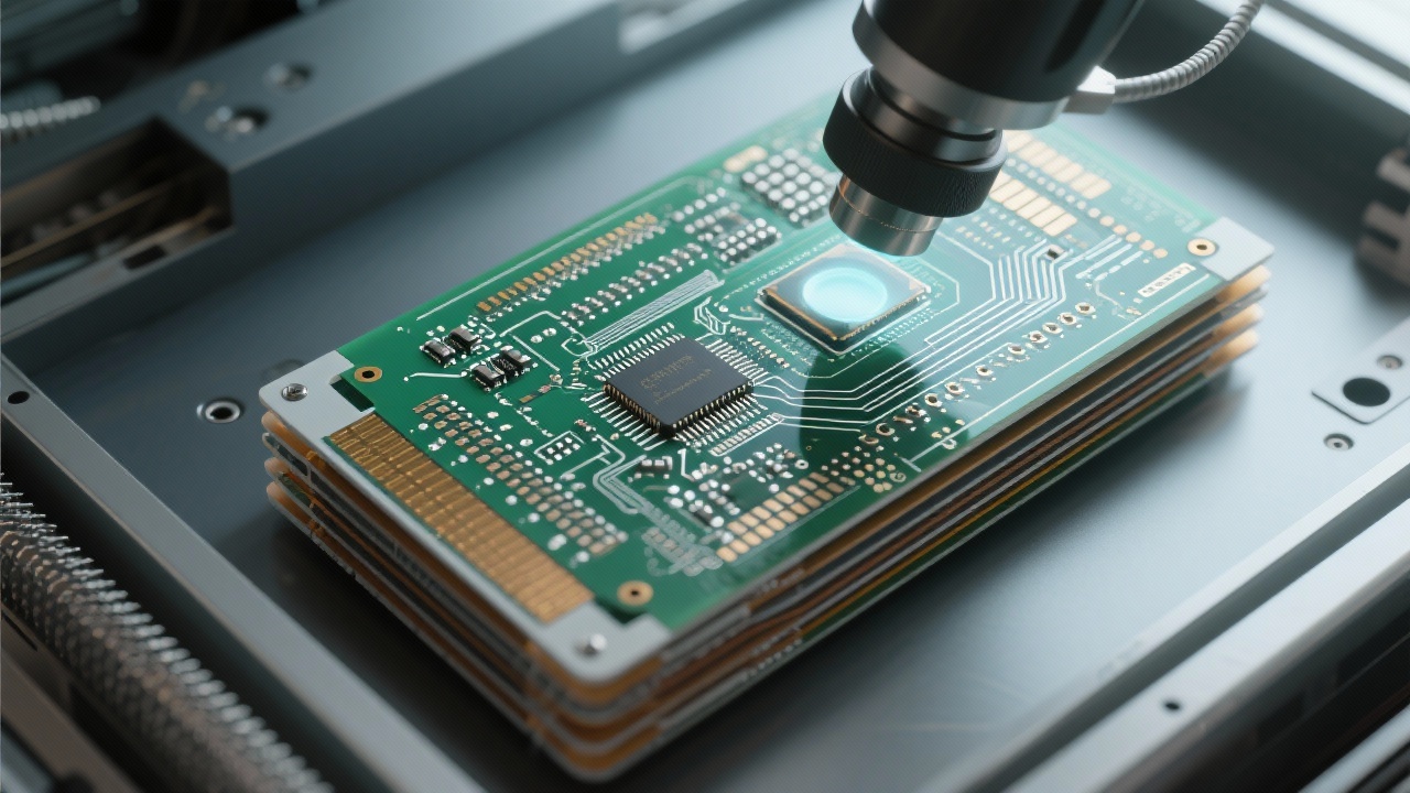
Flying probe testing technology is an essential non-contact method for validating electrical connectivity and detecting shorts or opens in the PCB. Utilizing computer-controlled spring-loaded probes guided by high-precision robotics, this testing ensures 100% coverage even for complex double-sided boards.
Compared to traditional bed-of-nails fixtures, flying probe testers reduce tooling costs dramatically and allow faster turnaround times—critical for rapid manufacturing environments. Typical probing speed can reach up to 1,200 test points per hour with accuracy margins within ±10 µm. Moreover, adaptable programs support iterative design changes without delay.
Companies investing in autonomous double-layer PCB production gain significant benefits including strict quality control, marked by first-pass yield improvements of up to 15%. Lead times can shrink from industry averages of 20–25 days down to 7–10 days through streamlined process integration. These efficiencies boost responsiveness amid fluctuating market demands.
In-house capabilities also facilitate tailored process optimizations according to client-specific requirements. For example, adjustments in lamination protocols or surface finish selections can be promptly implemented, ensuring enhanced product reliability and customer satisfaction.
Effective manufacturing planning integrates real-time production tracking and inventory management, enabling dynamic scheduling responsive to order volumes and priority shifts. Utilizing lean manufacturing principles, setup times are minimized, and throughput is maximized without sacrificing quality.
Complemented by optimized logistics solutions, companies ensure quick global shipment and minimized transit risks. Typical end-to-end delivery performance often surpasses 95% on-time rates, a critical factor in supporting just-in-time assembly operations across diversified customer portfolios.
 402
|
402
|
 FPC Hochdichte-Leiterbahnen
flexible Schaltungstechnik
Leiterbahnabstand 0
1 mm
elektromagnetische Verträglichkeit
flexible Leiterplattenfertigung
142
|
Hochgeschwindigkeits-Mehrschicht-PCB
Impedanzkontrolle
Telekommunikations-Hochfrequenz-PCB
5G-Kommunikations-PCB
Signalintegrität
125
|
FPC Hochdichte Layout
flexible Leiterplatten Design
elektromagnetische Verträglichkeit Optimierung
Signalübersprechen Prävention
Mikrobohrungen FPC
274
|
Impedanzkontrolle Hochgeschwindigkeits-PCB
PCB Impedanzmessung
AOI Prüfverfahren
5G PCB Design
Hochfrequenz-Leiterplatten Fertigung
259
|
Impedanzkontrolle
Hochfrequenz-PCB
5G-Basisstation-PCB
Signalintegrität
Hochgeschwindigkeits-Mehrlagen-PCB
FPC Hochdichte-Leiterbahnen
flexible Schaltungstechnik
Leiterbahnabstand 0
1 mm
elektromagnetische Verträglichkeit
flexible Leiterplattenfertigung
142
|
Hochgeschwindigkeits-Mehrschicht-PCB
Impedanzkontrolle
Telekommunikations-Hochfrequenz-PCB
5G-Kommunikations-PCB
Signalintegrität
125
|
FPC Hochdichte Layout
flexible Leiterplatten Design
elektromagnetische Verträglichkeit Optimierung
Signalübersprechen Prävention
Mikrobohrungen FPC
274
|
Impedanzkontrolle Hochgeschwindigkeits-PCB
PCB Impedanzmessung
AOI Prüfverfahren
5G PCB Design
Hochfrequenz-Leiterplatten Fertigung
259
|
Impedanzkontrolle
Hochfrequenz-PCB
5G-Basisstation-PCB
Signalintegrität
Hochgeschwindigkeits-Mehrlagen-PCB


-4.png?x-oss-process=image/resize,m_fill,h_800,w_800/format,webp)
-L4-4.png?x-oss-process=image/resize,m_fill,h_800,w_800/format,webp)


-1.png?x-oss-process=image/resize,m_fill,h_800,w_800/format,webp)


