
In high-density application scenarios such as consumer electronics and medical devices, you may have encountered the challenges of signal integrity and mechanical reliability caused by dense wiring in limited spaces. The close proximity of traces can lead to signal crosstalk, and the stress concentration in bent areas may affect the long - term reliability of flexible printed circuits (FPCs). Our team has delved deep into these issues to find effective solutions.
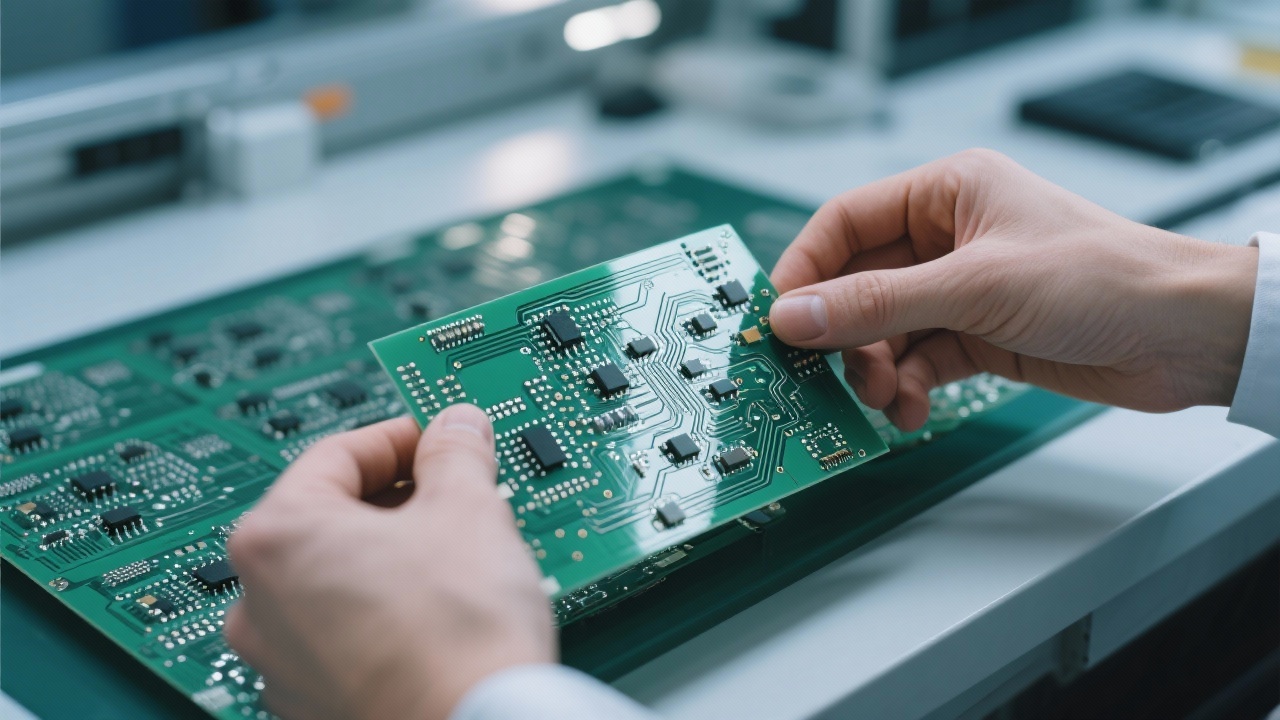
Layout optimization is crucial for high - density FPC design. By carefully arranging components and traces, we can reduce the risk of signal interference. For example, separating high - speed and low - speed signal traces can effectively improve signal integrity. Our engineers have developed a set of layout optimization algorithms based on years of experience, which can significantly enhance the performance of FPCs in high - density environments.
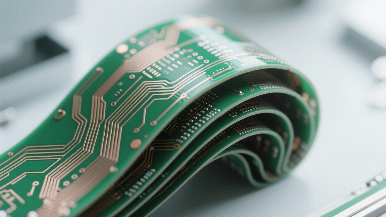
Controlling the trace spacing is another key factor. The minimum trace spacing in our high - density FPCs can reach 0.1mm. To achieve this, we use advanced manufacturing techniques and precise design tools. This allows for more traces to be placed in a limited space, increasing the overall functionality of the FPC. As shown in the following reference box, industry standards also emphasize the importance of proper trace spacing:
"In high - density FPC design, maintaining appropriate trace spacing is essential to ensure signal integrity and prevent crosstalk." - Industry Standard Specification
The via structure also has a significant impact on the performance of FPCs. Our research shows that the size and shape of vias can affect signal transmission and mechanical reliability. We have optimized our via design to minimize signal loss and improve the mechanical strength of FPCs in high - density applications.
Let's take a look at a typical customer project. A customer in the medical device industry needed a high - density FPC for their new product. By combining structure design, material selection, and process optimization, we successfully avoided signal crosstalk and component failure. The following is the feedback from the customer:
"Your team's solution has greatly improved the performance and reliability of our product. We are very satisfied with the results." - [Customer Name]
Our team has provided such customized solutions for more than 200 customers, demonstrating our strong technical strength and ability to solve complex problems.
We have the ability to achieve a minimum aperture of 0.2mm and a line width/space of 0.1mm/0.1mm. This high - precision manufacturing technology provides greater design freedom for engineers. With these capabilities, we can meet the most demanding requirements of high - density FPC design, enabling you to create more innovative products.
From the Design for Manufacturability (DFM) perspective, we understand how to accurately translate design intentions into the mass - production stage. Our engineers work closely with you throughout the entire process, from concept design to final production, ensuring that your high - density FPC design can be smoothly implemented.
Do you have any questions or challenges regarding high - density FPC design? Feel free to leave a comment below. We are always here to help you find the best solutions.
Explore Our High - Density FPC Solutions 291
|
291
|
 Hochgeschwindigkeits-Multilayer-PCB
Impedanzkontrolle
5G-Kommunikationsmodul
Hochfrequenz-PCB-Design
AOI-Test
459
|
FPC Via Design
FPC Biegebereich Spannungskonzentration
Flexibles Leiterplatten Design
Hochdichtverdrahtung
Signalintegrität FPC
41
|
Hochdichte Leiterbahnführung in FPCs
Entwurfstechniken für flexible Leiterplatten
Optimierung der elektromagnetischen Kompatibilität
Herstellungsprozesse für hochdichte flexible Leiterplatten
Mindestlochdurchmesser 0
2 mm
156
|
Flexible PCB Design
Multilayer FPC
Mikrolochverarbeitung
EMV-Optimierung
High-Density Interconnect
377
|
FPC Hochdichte-Bestückung
Flexible Leiterplatte Design
EMC-Optimierung Flex PCB
High-Density-FPC-Technik
FPC Herstellungstechnologie
Hochgeschwindigkeits-Multilayer-PCB
Impedanzkontrolle
5G-Kommunikationsmodul
Hochfrequenz-PCB-Design
AOI-Test
459
|
FPC Via Design
FPC Biegebereich Spannungskonzentration
Flexibles Leiterplatten Design
Hochdichtverdrahtung
Signalintegrität FPC
41
|
Hochdichte Leiterbahnführung in FPCs
Entwurfstechniken für flexible Leiterplatten
Optimierung der elektromagnetischen Kompatibilität
Herstellungsprozesse für hochdichte flexible Leiterplatten
Mindestlochdurchmesser 0
2 mm
156
|
Flexible PCB Design
Multilayer FPC
Mikrolochverarbeitung
EMV-Optimierung
High-Density Interconnect
377
|
FPC Hochdichte-Bestückung
Flexible Leiterplatte Design
EMC-Optimierung Flex PCB
High-Density-FPC-Technik
FPC Herstellungstechnologie


-4.png?x-oss-process=image/resize,m_fill,h_800,w_800/format,webp)


