
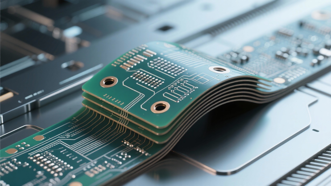
In the era of rapid development of electronic technology, multi - layer flexible printed circuit boards (FPCs) have become crucial components in various electronic devices, especially in consumer electronics and medical equipment where space is extremely limited. This article delves deep into the via design challenges in high - density wiring of multi - layer FPCs and the corresponding manufacturing process support.
The high - density wiring of FPCs involves several core technical difficulties. Firstly, layout optimization is of great importance. Engineers need to make full use of limited space to arrange circuits reasonably. For example, in a smartphone, the FPC needs to connect various components such as the screen, camera, and motherboard. A well - optimized layout can reduce the length of the circuit, thereby improving signal transmission efficiency.
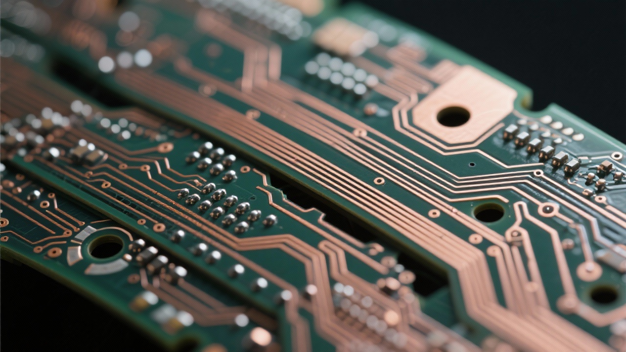
Secondly, controlling the line width and spacing is a key challenge. The minimum line width and spacing can reach 0.1mm. This requires high - precision manufacturing equipment and strict quality control. According to industry statistics, a deviation of even 0.01mm in line width or spacing can lead to signal interference or short - circuit problems in about 10% of cases.
Via design is also a critical aspect. Different via structures have different impacts on signal integrity and electromagnetic compatibility. For single - sided, double - sided, and multi - layer FPCs, the design principles of vias vary. A reasonable via design can effectively avoid signal crosstalk and stress concentration.
To address the issue of signal crosstalk, specific measures can be taken. For instance, by increasing the distance between signal lines or using shielding layers, the interference between signals can be reduced. In a real - world case of a medical monitoring device, through the use of shielding layers, the signal crosstalk rate was reduced from 8% to less than 2%.
Improving electromagnetic compatibility is also essential. This can be achieved by optimizing the circuit layout and using appropriate materials. For example, using materials with good electromagnetic shielding properties can effectively reduce electromagnetic interference. In the field of consumer electronics, products with excellent electromagnetic compatibility are more likely to meet international standards and gain market competitiveness.
In the folding area of FPCs, stress and reliability are major concerns. By using special materials and structures, such as flexible materials with high tensile strength and optimized folding angles, the reliability of the folding area can be improved. According to experimental data, after using these improvement measures, the service life of the folding area can be extended by about 30%.
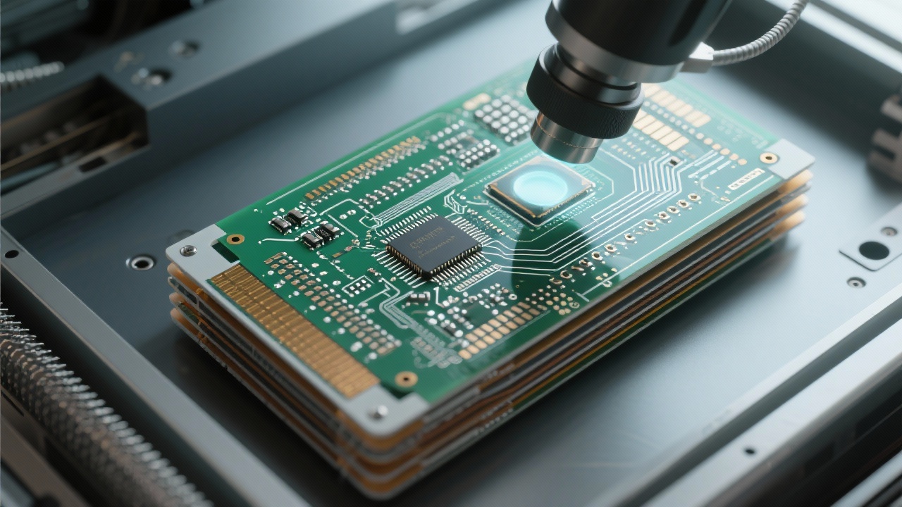
The manufacturing process of FPCs is also a key factor in ensuring high - quality products. Our company has advanced manufacturing technology, with a precision machining ability of a minimum hole diameter of 0.2mm. This allows us to support the implementation of complex designs. From design principles to mass - production implementation, we provide a full - process technical support.
In the manufacturing process, we strictly follow industry standards and the latest technological trends. Through continuous innovation and improvement, we can ensure the stability and reliability of product quality. Our products have been widely recognized in the market for their high quality and excellent performance.
If you are looking for high - quality flexible circuit board solutions, our company can provide you with professional technical support and reliable service. We are committed to helping you solve various problems in FPC design and manufacturing. Click here to learn more about our high - quality flexible circuit board solutions!
 402
|
402
|
 FPC Hochdichte-Leiterbahnen
flexible Schaltungstechnik
Leiterbahnabstand 0
1 mm
elektromagnetische Verträglichkeit
flexible Leiterplattenfertigung
291
|
Hochgeschwindigkeits-Multilayer-PCB
Impedanzkontrolle
5G-Kommunikationsmodul
Hochfrequenz-PCB-Design
AOI-Test
412
|
Doppelschicht-PCB
Schnellfertigung von PCB
Oberflächenbehandlungstechnologie
Flying-Probe-Test
PCB-Produktionsprozess
317
|
FPC Hochdichtebestückung
flexible Leiterplatte Design
EMV Optimierung
medizinische FPC
hochdichte flexible PCB
377
|
FPC Hochdichte-Bestückung
Flexible Leiterplatte Design
EMC-Optimierung Flex PCB
High-Density-FPC-Technik
FPC Herstellungstechnologie
FPC Hochdichte-Leiterbahnen
flexible Schaltungstechnik
Leiterbahnabstand 0
1 mm
elektromagnetische Verträglichkeit
flexible Leiterplattenfertigung
291
|
Hochgeschwindigkeits-Multilayer-PCB
Impedanzkontrolle
5G-Kommunikationsmodul
Hochfrequenz-PCB-Design
AOI-Test
412
|
Doppelschicht-PCB
Schnellfertigung von PCB
Oberflächenbehandlungstechnologie
Flying-Probe-Test
PCB-Produktionsprozess
317
|
FPC Hochdichtebestückung
flexible Leiterplatte Design
EMV Optimierung
medizinische FPC
hochdichte flexible PCB
377
|
FPC Hochdichte-Bestückung
Flexible Leiterplatte Design
EMC-Optimierung Flex PCB
High-Density-FPC-Technik
FPC Herstellungstechnologie


-L4-4.png?x-oss-process=image/resize,m_fill,h_800,w_800/format,webp)

-1.png?x-oss-process=image/resize,m_fill,h_800,w_800/format,webp)

-4.png?x-oss-process=image/resize,m_fill,h_800,w_800/format,webp)
-4.png?x-oss-process=image/resize,h_800,m_lfit/format,webp)

-1.png?x-oss-process=image/resize,h_800,m_lfit/format,webp)


