Mastering Thick Copper Etching: Achieving Uniformity and Precision for 4oz+ PCBs in Power Electronics

Ruiheng PCB
2026-03-02
Tutorial Guide
This technical guide delves into the critical challenges of thick copper layer etching in high-performance PCB manufacturing—particularly for 4 ounces per square foot (oz/ft²) and above. It explores solutions for uniform etching, high-precision trace design, and avoiding copper lift-off deformation. Key processes such as solder mask selection and application are detailed to ensure long-term stability under thermal and mechanical stress. The article also covers advanced drilling techniques for 0.5mm minimum hole sizes, essential for reliable electrical and mechanical connections. Supported by industry-standard data, process flow diagrams, and real-world case studies, this resource offers actionable insights for PCB engineers and quality professionals aiming to improve yield, consistency, and performance in power electronics applications.
https://shmuker.oss-accelerate.aliyuncs.com/data/oss/20251230/ad1efdc43fb7ec87673b41226508fc2d/ca4a2711-4cda-4529-a7a3-1efe9c8f1ada.jpeg

Mastering Thick Copper Etching: Achieving Uniformity and Precision in High-Performance PCBs

When designing power electronics PCBs, one of the most critical challenges engineers face is achieving consistent etching on copper layers exceeding 4 oz/ft²—especially when precision routing and mechanical durability are non-negotiable. This guide dives deep into real-world technical hurdles and proven solutions used by leading manufacturers to produce high-reliability thick copper PCBs for industrial, automotive, and renewable energy applications.

Why 4+ Oz Copper Layers Demand Specialized Processes

Standard etching methods often fail at 4 oz (137 µm) or higher due to uneven chemical reaction rates across thick copper profiles. According to IPC-4562 standards, non-uniform etch depth can exceed ±15% without optimized process control. To maintain circuit integrity, advanced techniques like pulsed current etching and multi-stage developer chemistry must be implemented. For instance, a case study from a Tier-1 EV supplier showed that switching from conventional batch etching to continuous flow etching improved yield from 82% to 96% on 6 oz copper boards.

Blocking the Unwanted: Advanced Solder Mask Selection

The choice of solder mask directly impacts long-term thermal and mechanical stability. Epoxies with low Tg values (<120°C) may delaminate under repeated thermal cycling—a common issue in motor drives and inverters. We recommend using UV-curable acrylics or polyimide-based masks rated for >180°C operating temps. A comparative test conducted by UMC demonstrated that polyimide masks retained adhesion after 500 thermal shock cycles (−40°C to +150°C), while standard epoxy failed at cycle 250.

Illustration showing cross-section of thick copper PCB with uniform etching and robust solder mask layer

Precision Drilling: Pushing the Limits to 0.5mm Holes

As board densities increase, drilling holes as small as 0.5 mm becomes essential—not just for signal integrity but also for mechanical anchoring in vibration-prone environments. Using laser drilling instead of mechanical drills reduces burr formation by up to 70%, per a 2023 report from PCDM. Additionally, implementing automated drill path optimization software ensures hole-to-hole positional accuracy within ±0.02 mm—critical for high-density surface mount assembly.

Quality Control That Matters: From Process Monitoring to Final Inspection

Top-tier manufacturers now integrate inline AOI (Automated Optical Inspection) systems with real-time data logging. These tools catch defects early—like partial etching or microcracks in solder mask—before they escalate. One European PCB maker reported a 40% reduction in rework costs after deploying AI-powered AOI that flagged anomalies based on historical failure patterns.

Flowchart illustrating the complete thick copper PCB manufacturing process from raw material to final inspection

If your project demands reliable performance under extreme conditions—whether it’s high current, frequent thermal stress, or harsh mechanical environments—your PCB partner must go beyond basic capabilities. At Shengyi, we specialize in thick copper PCBs with ENIG finish, capable of handling 6 oz copper, 0.5 mm vias, and over 1000 hours of thermal cycling without degradation.

Name *
Email *
Message*

Recommended Products

Related Reading

Dual-Layer PCB Rapid Manufacturing Process: From Design to Flying Probe Testing Explained

2026-02-04 | https://shmuker.oss-accelerate.aliyuncs.com/tmp/temporary/60ec5bd7f8d5a86c84ef79f2/60ec5bdcf8d5a86c84ef7a9a/20240305161110/eye.png 88 | https://shmuker.oss-accelerate.aliyuncs.com/tmp/temporary/60ec5bd7f8d5a86c84ef79f2/60ec5bdcf8d5a86c84ef7a9a/20240305160636/lable.png dual layer pcb manufacturing flying probe test surface finish options pcb rapid prototyping pcb production process

FPC High-Density Routing: Key Techniques for Layout Optimization and Trace Spacing Control

2026-01-05 | https://shmuker.oss-accelerate.aliyuncs.com/tmp/temporary/60ec5bd7f8d5a86c84ef79f2/60ec5bdcf8d5a86c84ef7a9a/20240305161110/eye.png 249 | https://shmuker.oss-accelerate.aliyuncs.com/tmp/temporary/60ec5bd7f8d5a86c84ef79f2/60ec5bdcf8d5a86c84ef7a9a/20240305160636/lable.png 
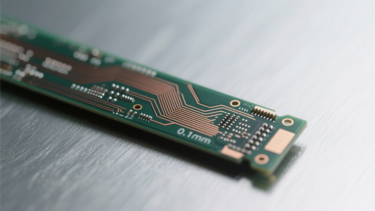
FPC high-density routing flexible circuit board design trace spacing control EMI shielding in FPC flexible PCB manufacturing

Why 0.5% PCB Warpage Is the New Benchmark for High-End HDI Boards Under IPC Standards

2026-02-19 | https://shmuker.oss-accelerate.aliyuncs.com/tmp/temporary/60ec5bd7f8d5a86c84ef79f2/60ec5bdcf8d5a86c84ef7a9a/20240305161110/eye.png 126 | https://shmuker.oss-accelerate.aliyuncs.com/tmp/temporary/60ec5bd7f8d5a86c84ef79f2/60ec5bdcf8d5a86c84ef7a9a/20240305160636/lable.png 0.5% PCB warpage HDI PCB flatness control IPC PCB warpage limit semiconductor test PCB high-end HDI PCB export quality

5G Base Station PCB Design: Impedance Matching Success Case Study & Practical Guide

2026-01-26 | https://shmuker.oss-accelerate.aliyuncs.com/tmp/temporary/60ec5bd7f8d5a86c84ef79f2/60ec5bdcf8d5a86c84ef7a9a/20240305161110/eye.png 154 | https://shmuker.oss-accelerate.aliyuncs.com/tmp/temporary/60ec5bd7f8d5a86c84ef79f2/60ec5bdcf8d5a86c84ef7a9a/20240305160636/lable.png 5G PCB design impedance control high-frequency communication modules high-speed multilayer PCB signal integrity

Recommended Flexible Circuit Board Solutions with the Latest FPC High-Density Wiring Technology

2026-01-09 | https://shmuker.oss-accelerate.aliyuncs.com/tmp/temporary/60ec5bd7f8d5a86c84ef79f2/60ec5bdcf8d5a86c84ef7a9a/20240305161110/eye.png 96 | https://shmuker.oss-accelerate.aliyuncs.com/tmp/temporary/60ec5bd7f8d5a86c84ef79f2/60ec5bdcf8d5a86c84ef7a9a/20240305160636/lable.png FPC high - density wiring Flexible circuit board design techniques Electromagnetic compatibility optimization High - density flexible PCB Multi - layer FPC manufacturing process
Popular articles
https://shmuker.oss-accelerate.aliyuncs.com/data/oss/20251230/76402db4ddda640df1d8ea772a31c807/0ec0487d-c513-4ae1-bddb-49f7de806bce.jpeg
https://shmuker.oss-accelerate.aliyuncs.com/data/oss/20251230/10162eed1c55dc9d2c2f47a0acfd4f76/514a91c4-e6c4-488d-a6e8-0a112d4b66b7.jpeg
https://shmuker.oss-accelerate.aliyuncs.com/data/oss/20251230/74cae3ecdb9a0b7f18e44f6631cea9fa/a50611de-8ff5-4f46-a7e1-6a2a52b90b99.jpeg
https://shmuker.oss-accelerate.aliyuncs.com/data/oss/20251230/108753c856212ca24423e047f1fae39d/aaca0d0a-903c-4a00-8d92-9c30893b54c5.jpeg
https://shmuker.oss-accelerate.aliyuncs.com/data/oss/20251230/5c69fdd5ace28e3cea2fb4c117e4557a/b1df2e5c-4f37-4544-a170-ad2d4e887ce0.jpeg
https://shmuker.oss-accelerate.aliyuncs.com/data/oss/692910f1af15994642dab58b/692a498eaf15994642dace1b/20251216152709/24-layer-circuit-board-4.png
https://shmuker.oss-accelerate.aliyuncs.com/data/oss/20251230/8b8b1d37b71e344d6a5f246185ce2506/34fa0194-4837-4f46-a9a0-4f56a966047d.jpeg
https://shmuker.oss-accelerate.aliyuncs.com/data/oss/20251230/ad1efdc43fb7ec87673b41226508fc2d/ca4a2711-4cda-4529-a7a3-1efe9c8f1ada.jpeg
https://shmuker.oss-accelerate.aliyuncs.com/data/oss/20251230/76402db4ddda640df1d8ea772a31c807/0ec0487d-c513-4ae1-bddb-49f7de806bce.jpeg
https://shmuker.oss-accelerate.aliyuncs.com/data/oss/20251230/5c69fdd5ace28e3cea2fb4c117e4557a/b1df2e5c-4f37-4544-a170-ad2d4e887ce0.jpeg
Recommended Reading
Contact us
Contact us
https://shmuker.oss-accelerate.aliyuncs.com/tmp/temporary/60ec5bd7f8d5a86c84ef79f2/60ec5bdcf8d5a86c84ef7a9a/thumb-prev.png