
In semiconductor test systems—ATE load boards, probe interface boards, and high-pin-count socket adapters—signal integrity is rarely limited by “one big issue.” More often, it is the cumulative effect of small discontinuities: via stubs, copper thickness variation, resin recession, and drill-to-pad misregistration. Within this reality, two parameters repeatedly separate stable test performance from noisy, drifting results: 0.30 mm-class microvia structures and a controlled 17:1 via aspect ratio in thick, multi-layer HDI stacks (e.g., 34 layers).
This article explains what these numbers actually mean in manufacturing terms, why they influence impedance continuity, crosstalk, and assembly reliability, and how process controls—laser drilling accuracy, backdrill depth control, and copper uniformity—work together under real test-board constraints.
A 0.30 mm microvia (often used as a practical boundary between standard mechanical microvias and finer laser-defined structures, depending on the stack design) is not simply a routing convenience. It changes the electromagnetic and mechanical behavior of the interconnect. Smaller via barrels typically reduce parasitic capacitance and help control return-current paths, especially where dense escape routing forces tighter reference-plane transitions.
The via aspect ratio—commonly defined as board thickness ÷ finished hole diameter for through holes—becomes critical in thick HDI stacks used in high-layer-count test boards. At 17:1, plating distribution, wall roughness, and void risk rise sharply if drilling, desmear, and copper deposition are not tightly controlled. In other words, aspect ratio is not just a “DFM number”; it is a direct proxy for plating reliability and electrical repeatability.
Practical reference: In high-speed digital links above ~10–16 Gbps, via stubs and impedance discontinuities can produce measurable reflections. Many teams target < 10% impedance deviation across transitions and keep effective via stubs under 0.3–0.5 mm in critical nets (actual targets vary by architecture and equalization).
In a 34-layer HDI build, the stack-up may combine sequential lamination, buried via structures, and selective through-hole strategies. The tighter the geometry, the narrower the process window. Three manufacturing realities dominate:
For small vias, a few tens of microns of misregistration can reduce annular ring margin and increase the probability of breakout—especially after multiple lamination cycles. Modern HDI lines typically hold laser drill positional accuracy around ±15–25 µm (equipment and material dependent), but the effective result depends on layer-to-layer movement and glass weave behavior. Cleaner hole walls also reduce copper roughness and improve plating uniformity.
At 17:1, insufficient throwing power can leave the via center under-plated compared to the knee and surface area. This matters electrically (resistance variation and local impedance change) and mechanically (fatigue cracking risk under thermal cycling). For mission-critical test fixtures that see repeated temperature sweeps, plating quality becomes a lifetime variable—not a one-time acceptance metric.
Copper distribution across planes and signal layers affects impedance more than many teams expect. A change of ±8–12 µm in outer-layer copper (after plating + etch) can shift controlled impedance traces by several ohms depending on geometry. In HDI, where line widths may be narrow, these variations compound. Tight control of copper thickness and dielectric spacing is therefore a direct signal-integrity control lever.
Laser-defined vias reduce the need for oversized pads and can keep interconnect transitions tighter, supporting denser escape routing around BGAs and high-density connectors. In high-speed nets, reducing the effective via pad and antipad discontinuity can help stabilize insertion loss and return loss, especially when combined with consistent reference-plane design.
Backdrilling is often the difference between a “works in the lab” board and a “holds margin across lots” test interface. Depth control is crucial: many production programs target ±75–100 µm backdrill depth tolerance, with verification via cross-section sampling. Removing unused via barrel length reduces resonant behavior and mitigates reflection peaks that otherwise appear in TDR and VNA measurements.
Test boards often carry a mix of RF-like fast edges, dense power delivery networks, and sensitive analog measurement traces. Copper thickness and etch consistency influence both trace impedance and plane impedance. Process strategies such as pattern plating optimization, local copper balancing, and controlled etch compensation reduce lot-to-lot variability—directly improving test repeatability.
When edge rates shorten and channel budgets tighten, the board interconnect must behave more like a controlled RF structure. In semiconductor testing, instability is often experienced as ATE margin shrink, intermittent bin shifts, or correlation gaps across sockets and sites. Properly executed 0.30 mm-class microvias and controlled high-aspect-ratio vias support three outcomes:
In practice, teams often report that disciplined stub control and uniform copper distribution reduce site-to-site variation and improve correlation—particularly when mixed-signal measurements are sensitive to reference noise and return-path discontinuities.
Consider a 34-layer semiconductor test board supporting high-speed digital lanes alongside precision measurement lines. A prior revision used conventional through-hole strategies with longer stubs and less controlled plating distribution in thicker sections. During bring-up, engineers observed inconsistent eye margins across sites and higher-than-expected crosstalk bursts in dense routing regions.
After redesigning the interconnect strategy to emphasize 0.30 mm-class microvia transitions, implementing systematic backdrilling on long through paths, and tightening process control on copper thickness uniformity, the next build showed:
The key takeaway is not that one single change “fixed everything,” but that the combination of geometry and process control reduced the cumulative interconnect uncertainty—exactly what high-volume or multi-site testing depends on.
Traditional multilayer PCBs can be cost-effective for general electronics, but semiconductor test boards create a harsher combination: thick stacks, dense interconnect, repeated assembly, and frequent thermal excursions. In this context, older approaches tend to struggle with:
Many test programs align quality expectations with widely recognized frameworks such as IPC-6012 (qualification and performance for rigid PCBs) and IPC-A-600 (acceptability of printed boards). For HDI-specific structures, teams often reference IPC-6016 to define acceptance criteria and workmanship expectations. These standards do not replace good design—but they establish the inspection language needed to keep complex builds under control.
The trajectory is clear: higher pin counts, faster interfaces, and more demanding correlation requirements push test boards toward tighter interconnect control. Near-term evolution typically includes more selective via strategies, broader adoption of backdrill on critical nets, and deeper reliance on statistical process control for copper and dielectric parameters.
At the same time, the most effective engineering organizations treat manufacturability and measurement as part of the design loop—building coupons that reflect real routing, requiring cross-section evidence on critical structures, and linking board acceptance to objective SI metrics.
 220
|
220
|
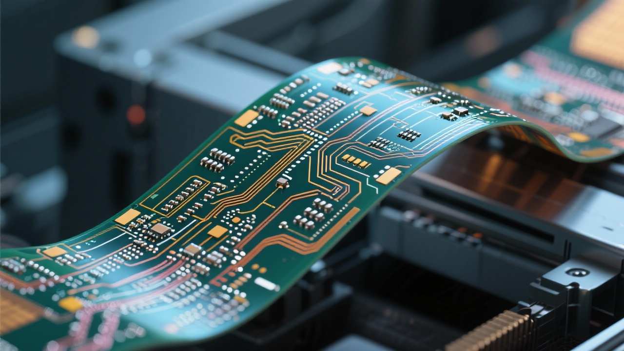
 FPC high - density routing
Flexible circuit board design techniques
Electromagnetic compatibility optimization
High - density routing solutions
Flexible PCB manufacturing processes
361
|
High-density FPC routing
Flexible circuit board design
Electromagnetic compatibility optimization
Precision FPC manufacturing
Flexible PCB reliability
315
|
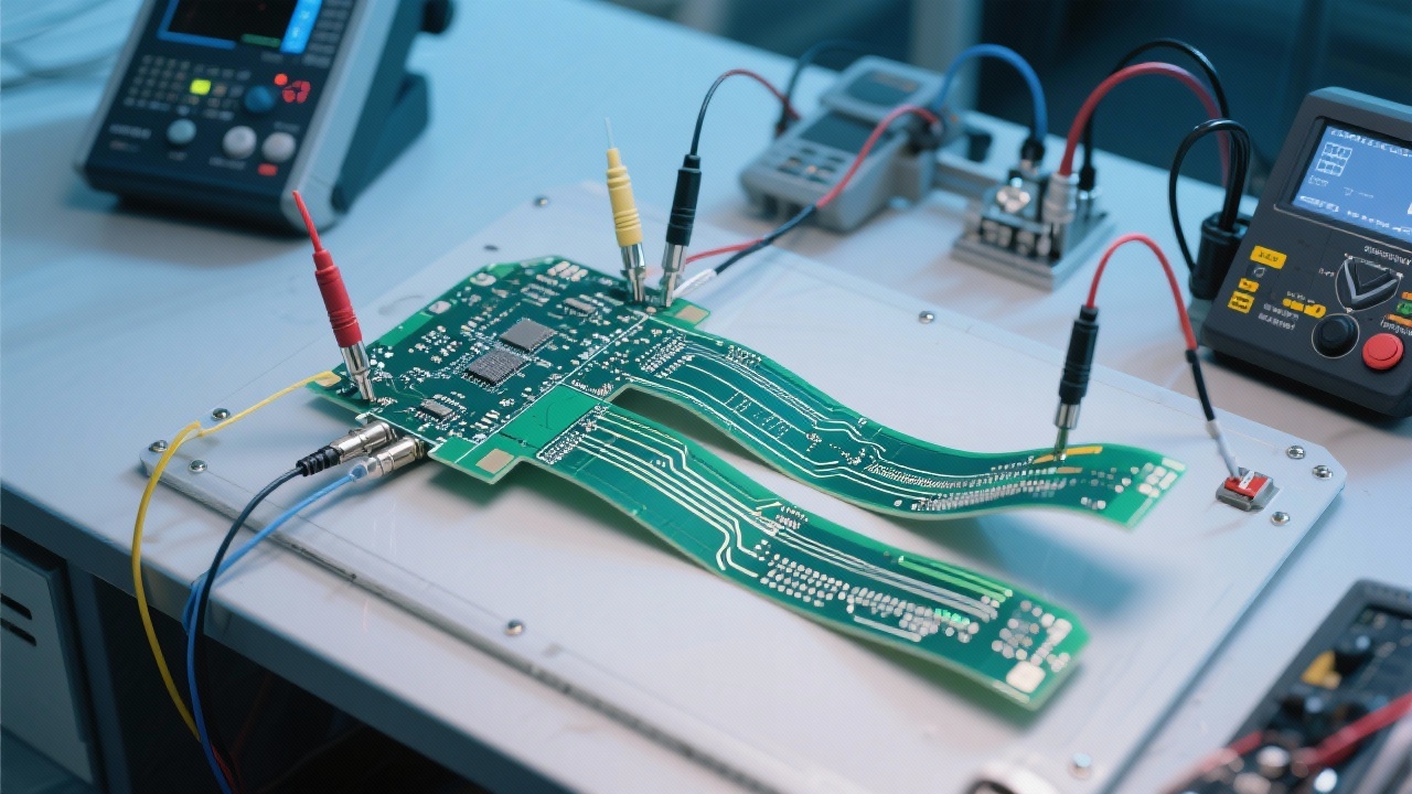
High-speed multilayer PCB
Impedance control technology
AOI detection
Signal integrity
5G communication PCB
145
|
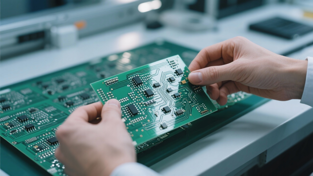
high-speed multilayer PCB impedance control
50 ohm single-ended impedance
100 ohm differential impedance
high-frequency PCB design
signal integrity optimization
325
|
FPC high - density wiring
Flexible circuit board design skills
Via design challenges
Electromagnetic compatibility optimization
Flexible PCB manufacturing process
FPC high - density routing
Flexible circuit board design techniques
Electromagnetic compatibility optimization
High - density routing solutions
Flexible PCB manufacturing processes
361
|
High-density FPC routing
Flexible circuit board design
Electromagnetic compatibility optimization
Precision FPC manufacturing
Flexible PCB reliability
315
|
High-speed multilayer PCB
Impedance control technology
AOI detection
Signal integrity
5G communication PCB
145
|
high-speed multilayer PCB impedance control
50 ohm single-ended impedance
100 ohm differential impedance
high-frequency PCB design
signal integrity optimization
325
|
FPC high - density wiring
Flexible circuit board design skills
Via design challenges
Electromagnetic compatibility optimization
Flexible PCB manufacturing process


-1.png?x-oss-process=image/resize,h_800,m_lfit/format,webp)


-L4-4.png?x-oss-process=image/resize,m_fill,h_800,w_800/format,webp)
-4.png?x-oss-process=image/resize,m_fill,h_800,w_800/format,webp)


