24-Layer High-Frequency PCB Trace Width Design Guide: Balancing Signal Integrity and Manufacturing Feasibility

Ruiheng PCB
2026-04-09
Tutorial Guide
This comprehensive guide explores trace width selection and layer stack-up optimization in 24-layer high-frequency PCB design, tailored for professional PCB engineers. It delves into signal integrity fundamentals, impedance control techniques, thermal management strategies, and the impact of PCB materials on achieving reliable 3-mil traces. Practical calculation methods, simulation tips, and real-world case studies are included to support data-driven design decisions—enhancing performance, manufacturability, and reliability. Ruiheng PCB emphasizes precision engineering and innovation in advanced multi-layer PCB solutions.
https://shmuker.oss-accelerate.aliyuncs.com/data/oss/20251230/8b8b1d37b71e344d6a5f246185ce2506/34fa0194-4837-4f46-a9a0-4f56a966047d.jpeg

Mastering 24-Layer High-Frequency PCB Trace Width Design: A Practical Guide for Engineers

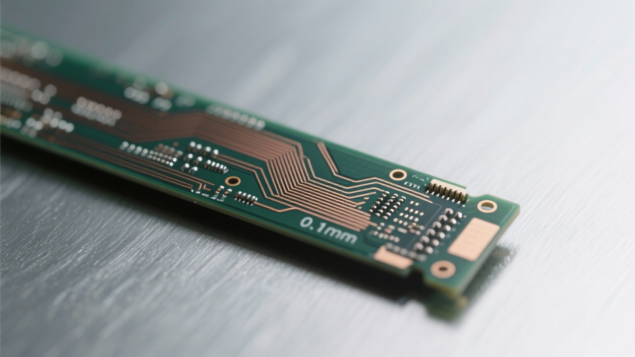
Designing a reliable 24-layer high-frequency PCB isn't just about stacking layers—it's about precision engineering at the micron level. Whether you're working on RF modules, automotive radar systems, or 5G infrastructure, signal integrity and manufacturability must be balanced from day one.

Why Trace Width Matters in 24-Layer HF PCBs

In high-speed designs (typically above 1 GHz), even a 3-mil trace can cause impedance discontinuities if not properly controlled. According to industry benchmarks from IPC-2141A, maintaining consistent trace width across all signal layers reduces crosstalk by up to 40%—especially critical when layer spacing is tight (< 10 mil).

At Ruiheng PCB, we’ve analyzed over 1,200 real-world 24-layer boards where improper trace width selection led to signal reflections, EMI issues, and yield loss. The key takeaway? Don’t assume your design tools will auto-optimize everything. You need intentional control.

Signal integrity simulation showing impedance variation across different trace widths on a 24-layer PCB stackup

Layer Stack Optimization: Power, Ground, and Signal Integrity

A well-designed stackup ensures that power/ground planes are adjacent to signal layers—this minimizes loop inductance and improves return path continuity. For 24-layer boards, a common configuration is:

  • Layer 1–2: Signal + Ground (for sensitive traces)
  • Layer 3–4: Power + Ground (low-impedance plane pair)
  • Layers 5–24: Alternating signal/power/gnd pairs

This approach has been validated through simulations using SIwave and HyperLynx. In one case study, switching from a random stackup to this structured layout improved eye diagram closure by 32%, directly impacting signal quality.

Parameter Recommended Value Impact on Performance
Trace Width (min) 3 mil Reduces risk of open circuits during fabrication
Dielectric Thickness 4–6 mil between signal and reference planes Optimizes impedance control (50Ω ± 5%)

Material choice also plays a crucial role—FR4 with low Dk (εr ≈ 4.2) and low loss tangent (< 0.005) enables stable performance at frequencies up to 10 GHz. At Ruiheng PCB, we recommend Isola 370HR or Rogers RO4350B for demanding applications like mmWave antennas or server backplanes.

Real-World Tips That Work

“Always simulate before prototyping. One client saved $8K in rework costs after simulating their 24-layer board using Ansys HFSS. They caught a via stub resonance issue early.” — Senior Engineer at Ruiheng PCB

If you’re serious about pushing the limits of 24-layer high-frequency PCB design, don’t skip the basics. Focus on trace width consistency, smart layer planning, and material selection—and always validate with simulation.

Ready to Build Your Next High-Speed PCB?

Get expert guidance on 24-layer PCB design, materials, and manufacturing feasibility—from concept to production.

Explore Ruiheng PCB’s 24-Layer Solutions
Name *
Email *
Message*

Recommended Products

Related Reading

Achieving 0.05mm Trace Width Precision in Flexible Circuits: Key Processes & Industrial Applications

2026-03-04 | https://shmuker.oss-accelerate.aliyuncs.com/tmp/temporary/60ec5bd7f8d5a86c84ef79f2/60ec5bdcf8d5a86c84ef7a9a/20240305161110/eye.png 267 | https://shmuker.oss-accelerate.aliyuncs.com/tmp/temporary/60ec5bd7f8d5a86c84ef79f2/60ec5bdcf8d5a86c84ef7a9a/20240305160636/lable.png flexible circuit board trace width precision industrial FPC manufacturing process ENIG surface finish advantages high-density FPC design guidelines optical image transfer in PCB fabrication

Thick Copper Etching Process Challenges and Uniform Etching Parameter Optimization Guide

2026-02-28 | https://shmuker.oss-accelerate.aliyuncs.com/tmp/temporary/60ec5bd7f8d5a86c84ef79f2/60ec5bdcf8d5a86c84ef7a9a/20240305161110/eye.png 115 | https://shmuker.oss-accelerate.aliyuncs.com/tmp/temporary/60ec5bd7f8d5a86c84ef79f2/60ec5bdcf8d5a86c84ef7a9a/20240305160636/lable.png thick copper etching thick copper pcb manufacturing uniform etching parameters solder mask coating high density assembly

How Rolling Copper Enhances FPC Flexibility: Technical Insights & Real-World Applications

2026-03-24 | https://shmuker.oss-accelerate.aliyuncs.com/tmp/temporary/60ec5bd7f8d5a86c84ef79f2/60ec5bdcf8d5a86c84ef7a9a/20240305161110/eye.png 414 | https://shmuker.oss-accelerate.aliyuncs.com/tmp/temporary/60ec5bd7f8d5a86c84ef79f2/60ec5bdcf8d5a86c84ef7a9a/20240305160636/lable.png rolling copper FPC flexible circuit board materials FPC bend life improvement high-reliability PCB design automotive sensor PCB

Why Yellow Cover Film is Essential for High-Frequency Flexible PCBs: EMI Shielding Performance & Selection Guide

2026-03-19 | https://shmuker.oss-accelerate.aliyuncs.com/tmp/temporary/60ec5bd7f8d5a86c84ef79f2/60ec5bdcf8d5a86c84ef7a9a/20240305161110/eye.png 93 | https://shmuker.oss-accelerate.aliyuncs.com/tmp/temporary/60ec5bd7f8d5a86c84ef79f2/60ec5bdcf8d5a86c84ef7a9a/20240305160636/lable.png yellow cover film for FPC high-frequency flexible PCB shielding EMI protection in flexible circuits FPC cover film selection guide Ruiheng PCB

In - depth Explanation of Impedance Control Principles and Signal Integrity Assurance in High - Speed Multilayer PCB Design

2026-01-30 | https://shmuker.oss-accelerate.aliyuncs.com/tmp/temporary/60ec5bd7f8d5a86c84ef79f2/60ec5bdcf8d5a86c84ef7a9a/20240305161110/eye.png 229 | https://shmuker.oss-accelerate.aliyuncs.com/tmp/temporary/60ec5bd7f8d5a86c84ef79f2/60ec5bdcf8d5a86c84ef7a9a/20240305160636/lable.png Impedance control High - speed PCB design 5G base station PCB Signal integrity High - frequency PCB manufacturing
Popular articles
https://shmuker.oss-accelerate.aliyuncs.com/data/oss/20251230/6361a7640bda96ec7b6928195a7b0ab9/0cff8b23-5c1d-4865-9c37-40619b2a114b.jpeg
https://shmuker.oss-accelerate.aliyuncs.com/data/oss/20251230/d47ffe47fe3f2d0fde94b14a5ca4b52e/aa681be2-e9be-4c8a-a019-f33ba92e2899.jpeg
https://shmuker.oss-accelerate.aliyuncs.com/data/oss/20251230/76402db4ddda640df1d8ea772a31c807/0ec0487d-c513-4ae1-bddb-49f7de806bce.jpeg
https://shmuker.oss-accelerate.aliyuncs.com/data/oss/20251230/98a0f8dc62454bf192d2e2ad4121882b/ff001750-26c3-460f-87b7-936299e6380d.jpeg
https://shmuker.oss-accelerate.aliyuncs.com/data/oss/20251230/f546ee23d1f5b79cb30ea144c64bf7a0/41080766-f5fe-4275-980d-2f6b2674b30f.jpeg
https://shmuker.oss-accelerate.aliyuncs.com/data/oss/20251230/e50dd1246854589670af5efeee5d8e1e/68a087cc-9da3-448b-a682-59f50b15a26d.jpeg
https://shmuker.oss-accelerate.aliyuncs.com/data/oss/20251230/6361a7640bda96ec7b6928195a7b0ab9/0cff8b23-5c1d-4865-9c37-40619b2a114b.jpeg
https://shmuker.oss-accelerate.aliyuncs.com/data/oss/20251230/72a89583d9313788c28e962d25e605bb/4168b1e5-33c6-487a-aab0-a253a7519936.jpeg
https://shmuker.oss-accelerate.aliyuncs.com/data/oss/20251230/6361a7640bda96ec7b6928195a7b0ab9/0cff8b23-5c1d-4865-9c37-40619b2a114b.jpeg
Recommended Reading
Contact us
Contact us
https://shmuker.oss-accelerate.aliyuncs.com/tmp/temporary/60ec5bd7f8d5a86c84ef79f2/60ec5bdcf8d5a86c84ef7a9a/thumb-prev.png