
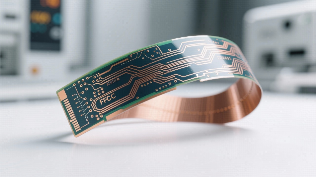
Flexible Printed Circuits (FPCs) are indispensable in high-density applications such as consumer electronics and medical devices. As devices become increasingly compact, optimizing electromagnetic compatibility (EMC) and mitigating signal crosstalk have emerged as pivotal to ensure both functional reliability and spatial efficiency. This article dissects key technical considerations in single-, double-, and multi-layer FPC layouts, targeting engineers seeking a data-driven approach to avoid electromagnetic interference (EMI) and manufacturing bottlenecks.
The densification of circuit layouts in constrained spaces often results in decreased trace spacing—commonly down to a minimal 0.1mm—which exponentially increases electromagnetic coupling risks. Such proximity leads to signal integrity degradation, manifested as crosstalk, noise, and overall EMC failures, jeopardizing product reliability especially in sensitive medical environments and critical consumer applications.
Effective layout design requires component placement that minimizes high-frequency signal paths near sensitive analog traces. By implementing dedicated ground planes and segregating noisy currents, designers reduce loop antennas responsible for EMI generation. Additionally, strategic layer stacking in multilayer FPCs can isolate signal and power layers to suppress electromagnetic coupling.
Standards recommend a minimum 0.1mm clearance between differential pairs to balance routing density and crosstalk reduction. Simultaneously, differential impedance matching across the 50Ω-100Ω range helps maintain signal integrity. Designers also prioritize orthogonal routing between adjacent layers to minimize capacitive coupling.
Employing microvias as small as 0.2mm diameter reduces parasitic inductance and capacitance effects. This facilitates compact vertical interconnections without compromising signal quality. Laser-drilled microvias enable complex multi-layer stacking, essential in advanced medical device PCBs demanding both miniaturization and high reliability.
In a recent medical monitoring device project, an observed 12% crosstalk-induced error rate was mitigated to under 1% by incorporating differential pair re-routing, ground shielding layers, and meticulous via placement. Verification tests confirmed compliance with EMC standards, underscoring the efficacy of rigorous design and iterative prototyping.
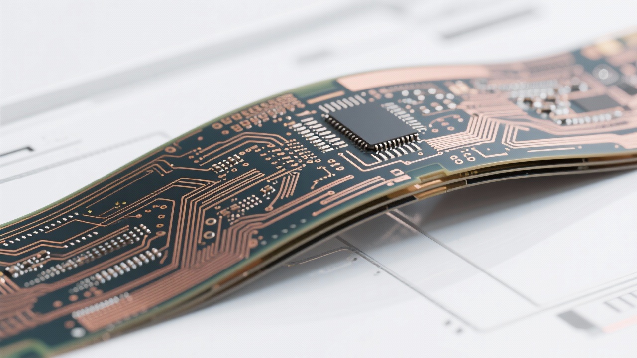
The successful realization of intricate FPC designs depends heavily on precise manufacturing technologies. Our manufacturing partners support advanced microvia drilling down to 0.2mm and line width/spacing as narrow as 0.1mm, enabling design integrity through reduced parasitic effects. These capabilities empower engineers to push density boundaries without compromising EMC performance or yield.
According to UL 94 and RoHS standards, materials and processes must mitigate flammability and hazardous substances, indirectly boosting electromagnetic integrity. Moreover, adherence to ISO 9001 ensures manufacturing consistency critical for EMC repeatability across production batches.

Engineering teams aiming to elevate their FPC projects' EMC robustness and manufacturability should embrace these proven design methodologies and partner with advanced fabrication experts. Our FPC solutions have been successfully integrated into cutting-edge medical devices, enabling compact form factors while ensuring the highest levels of signal integrity and EMC compliance.
 360
|
360
|
 High-density FPC routing
Flexible circuit board design
Electromagnetic compatibility optimization
Precision FPC manufacturing
Flexible PCB reliability
291
|
high-speed multilayer PCB
impedance control
5G communication module
high-frequency PCB design
signal integrity
459
|
Multilayer FPC Via Design
FPC Bend Area Stress
Flexible Circuit Design
High-Density FPC Routing
FPC Reliability Enhancement
412
|
double layer PCB rapid manufacturing
PCB surface finishing technologies
flying probe testing
PCB production process
electrical reliability testing
317
|
high-density FPC routing
flexible PCB design
EMI optimization
medical FPC
consumer electronics FPC
High-density FPC routing
Flexible circuit board design
Electromagnetic compatibility optimization
Precision FPC manufacturing
Flexible PCB reliability
291
|
high-speed multilayer PCB
impedance control
5G communication module
high-frequency PCB design
signal integrity
459
|
Multilayer FPC Via Design
FPC Bend Area Stress
Flexible Circuit Design
High-Density FPC Routing
FPC Reliability Enhancement
412
|
double layer PCB rapid manufacturing
PCB surface finishing technologies
flying probe testing
PCB production process
electrical reliability testing
317
|
high-density FPC routing
flexible PCB design
EMI optimization
medical FPC
consumer electronics FPC
-1.png?x-oss-process=image/resize,h_800,m_lfit/format,webp)


-4.png?x-oss-process=image/resize,m_fill,h_800,w_800/format,webp)


-L4-4.png?x-oss-process=image/resize,m_fill,h_800,w_800/format,webp)