
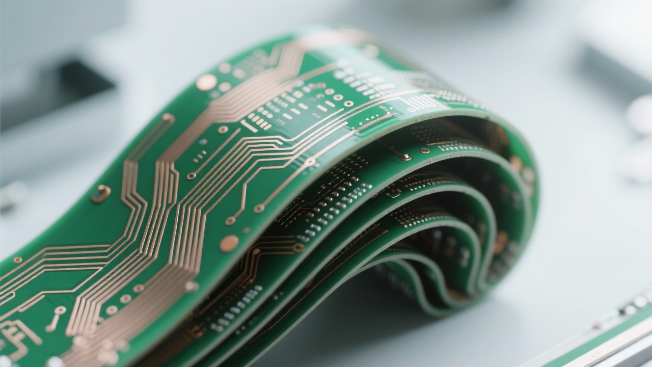
In the ever - evolving landscape of electronics, flexible printed circuit boards (FPCs) have become indispensable, especially in applications where space is at a premium. This article delves deep into the high - density routing technology in FPC design, offering comprehensive insights into the challenges and solutions for single - sided, double - sided, and multi - layer FPCs.
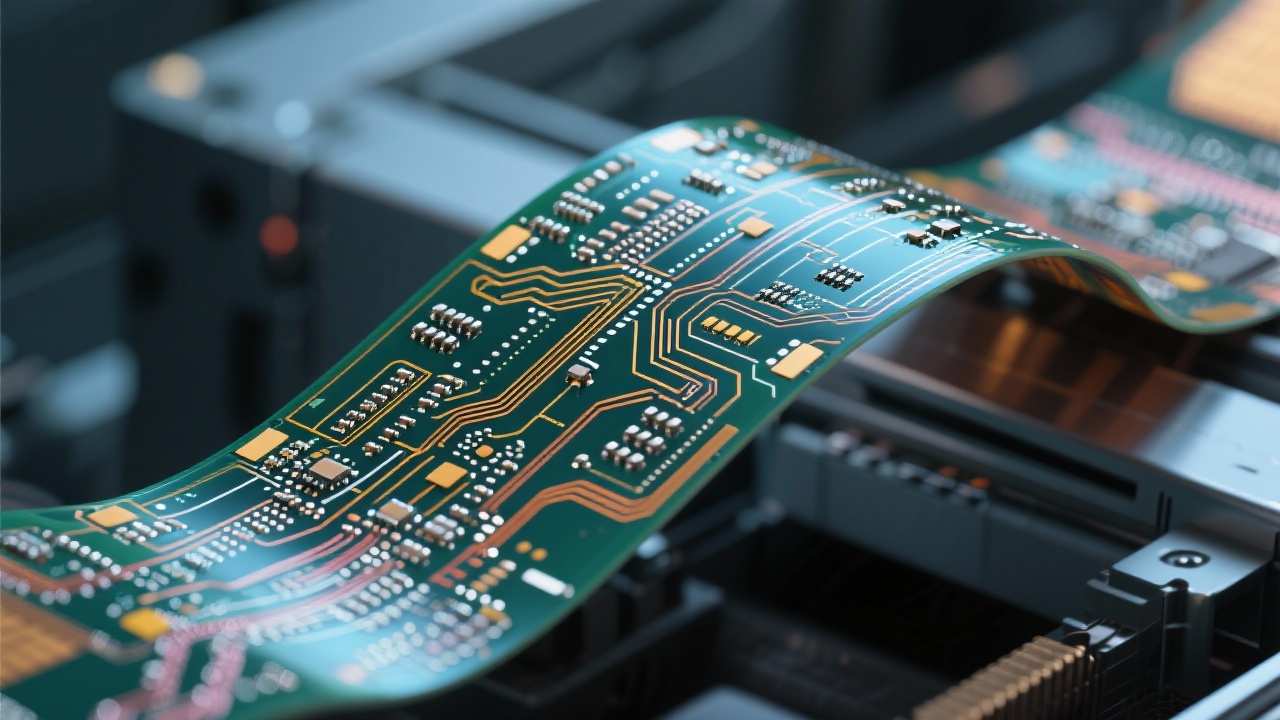
One of the primary challenges in FPC design is layout optimization. As the demand for smaller and more powerful devices grows, engineers need to pack more components into a limited space. For example, in modern smartphones, the FPCs must accommodate a large number of sensors, connectors, and other components. This requires precise control over the routing spacing, with a minimum of 0.1mm, to ensure proper signal transmission and prevent short - circuits.
Another crucial aspect is via design. The via, a small hole in the PCB that allows electrical connections between different layers, needs to be carefully designed. With the latest manufacturing processes, the minimum aperture for vias can reach 0.2mm, enabling more complex and compact designs.
Signal integrity is a major concern in high - density FPC design. In space - constrained applications such as wearables and medical devices, signal crosstalk can significantly degrade the performance of the device. To address this issue, engineers need to adopt effective crosstalk protection methods. For instance, by using proper shielding techniques and optimizing the routing patterns, the interference between signals can be minimized.
Electromagnetic compatibility (EMC) is also vital. In today's electromagnetic - rich environment, FPCs need to be designed to reduce electromagnetic interference (EMI) and ensure that the device can operate stably without affecting other nearby electronic devices. Through case studies in consumer electronics and medical equipment, this article explores various EMC optimization methods, such as using ferrite beads and proper grounding techniques.
The manufacturing process plays a crucial role in realizing complex FPC designs. Advanced techniques such as fine - line etching, which can control the line width and spacing accurately, and multi - layer lamination processes are essential. These processes ensure that the FPCs can meet the high - density requirements while maintaining high reliability.
For example, in a recent project for a medical monitoring device, the use of high - precision manufacturing processes allowed the FPC to integrate multiple sensors and communication modules in a very small form factor, improving the portability and functionality of the device.
Our company offers high - quality flexible printed circuit boards and a one - stop solution for FPC design and manufacturing. With years of experience and a team of expert engineers, we can help you overcome the challenges in FPC design and ensure seamless integration between design and production.

Whether you are designing a new consumer electronics product or a medical device, our solutions can enhance the efficiency of your FPC design and improve the reliability of your products. We are committed to providing you with the best support throughout the entire process.
Discover Our High - Quality FPC and One - Stop Solutions Now!
 402
|
402
|
 FPC high-density routing
flexible circuit board design tips
EMC optimization
high-density PCB trace spacing
flexible printed circuit manufacturing
125
|
high-density FPC layout
flexible PCB design techniques
electromagnetic compatibility optimization
signal crosstalk prevention
advanced flexible PCB manufacturing
459
|
Multilayer FPC Via Design
FPC Bend Area Stress
Flexible Circuit Design
High-Density FPC Routing
FPC Reliability Enhancement
41
|
FPC high-density wiring
Flexible circuit board design techniques
Electromagnetic compatibility optimization
High-density flexible PCB manufacturing process
Minimum hole diameter 0.2mm
325
|
FPC high - density wiring
Flexible circuit board design skills
Via design challenges
Electromagnetic compatibility optimization
Flexible PCB manufacturing process
FPC high-density routing
flexible circuit board design tips
EMC optimization
high-density PCB trace spacing
flexible printed circuit manufacturing
125
|
high-density FPC layout
flexible PCB design techniques
electromagnetic compatibility optimization
signal crosstalk prevention
advanced flexible PCB manufacturing
459
|
Multilayer FPC Via Design
FPC Bend Area Stress
Flexible Circuit Design
High-Density FPC Routing
FPC Reliability Enhancement
41
|
FPC high-density wiring
Flexible circuit board design techniques
Electromagnetic compatibility optimization
High-density flexible PCB manufacturing process
Minimum hole diameter 0.2mm
325
|
FPC high - density wiring
Flexible circuit board design skills
Via design challenges
Electromagnetic compatibility optimization
Flexible PCB manufacturing process


-1.png?x-oss-process=image/resize,m_fill,h_800,w_800/format,webp)

-L4-4.png?x-oss-process=image/resize,m_fill,h_800,w_800/format,webp)

-4.png?x-oss-process=image/resize,m_fill,h_800,w_800/format,webp)


