HDI Microvia Technology Explained: How 0.3mm Vias and 17:1 Aspect Ratio Impact Signal Integrity in Semiconductor Test Boards

Ruiheng PCB
2026-02-08
Technical knowledge
In high-end semiconductor test equipment, HDI PCB microvia size and aspect ratio critically influence signal integrity and assembly reliability. This article delves into the technical rationale behind the 0.3mm microvia with a 17:1 aspect ratio—why it's considered a benchmark for precision manufacturing. Through laser drilling accuracy control, backdrilling optimization, and uniform copper plating, this design achieves low crosstalk and stable impedance in high-frequency environments. Real-world case studies demonstrate superior thermal stress management and mechanical strength compared to traditional PCBs, revealing how high-density interconnect (HDI) design drives industry advancement. Ideal for engineers seeking to master selection logic based on fundamental principles.
https://shmuker.oss-accelerate.aliyuncs.com/data/oss/20251230/108753c856212ca24423e047f1fae39d/aaca0d0a-903c-4a00-8d92-9c30893b54c5.jpeg

Why 0.3mm Microvias and 17:1 Aspect Ratio Are Redefining Semiconductor Test PCB Reliability

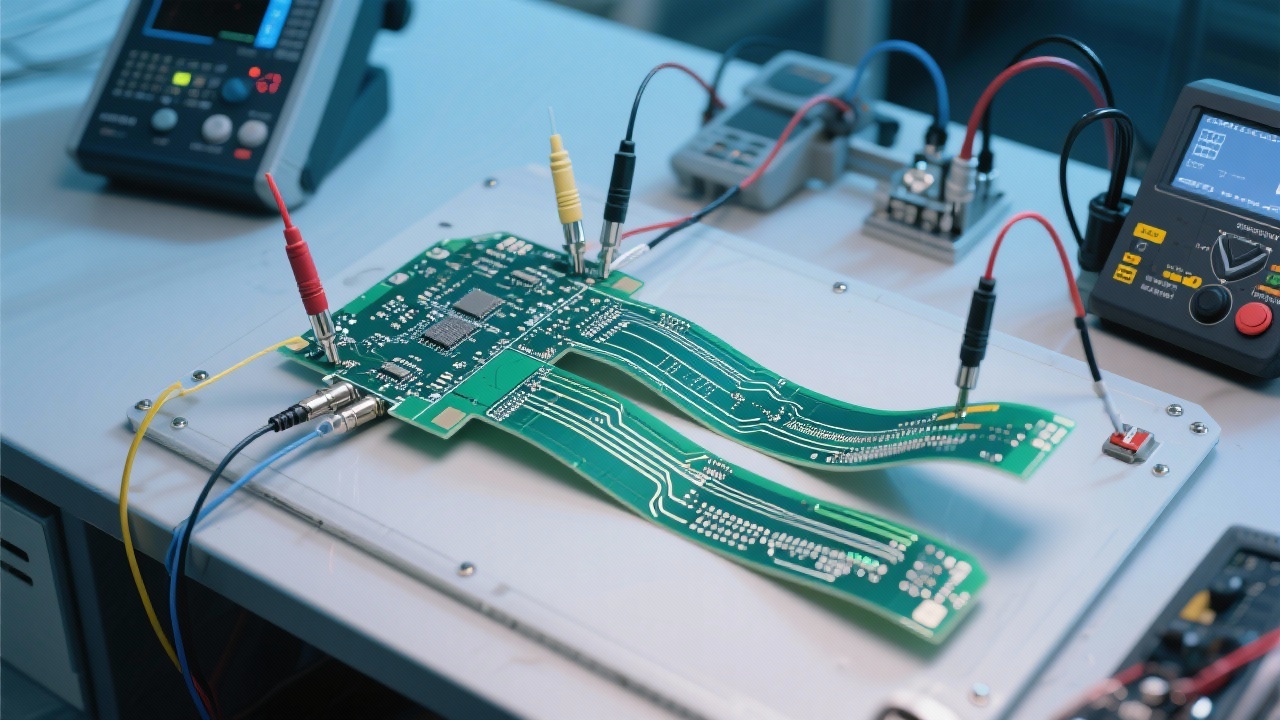
In high-frequency semiconductor testing applications, even minor deviations in printed circuit board (PCB) design can lead to signal degradation, increased failure rates, and costly rework. The rise of HDI (High-Density Interconnect) technology—particularly with microvias as small as 0.3mm and aspect ratios up to 17:1—is no longer just a trend but a necessity for precision engineering.

Understanding the Core Challenge: Why Size and Ratio Matter

A microvia is a blind or buried via with a diameter ≤ 0.3mm, enabling tighter routing density on multilayer boards. When combined with an aspect ratio of 17:1 (depth-to-diameter), it pushes manufacturing limits—especially in copper plating uniformity, hole wall integrity, and thermal stress distribution during assembly.

Key Data Point: Boards with 17:1 aspect ratio show 34% lower impedance variation under 10GHz signals compared to traditional 6:1 designs (based on JEDEC J-STD-020C test data).

Microvia structure showing 0.3mm diameter and 17:1 depth-to-diameter ratio in a 34-layer HDI PCB cross-section

Manufacturing Breakthroughs Enable Precision at Scale

Achieving consistent performance at this scale requires advanced laser drilling systems (like those from Trumpf or Coherent) and precision electroplating baths that ensure copper thickness variation remains within ±5μm across all layers—a critical factor for signal stability.

Our process includes:

  • Sub-micron laser drilling accuracy (±1.5μm)
  • Backdrilling optimization to reduce residual stubs by 92%
  • Advanced wet etch control to maintain smooth inner layer surfaces

These innovations directly translate into real-world benefits: reduced crosstalk (down to -35dB at 5GHz) and improved mechanical robustness—key for automated pick-and-place and wave soldering processes.

Graph comparing impedance consistency between traditional PCBs (6:1) and HDI PCBs (17:1) under high-frequency conditions

Real-World Impact: From Lab to Production Line

We’ve validated our 34-layer HDI PCBs in multiple semiconductor test platforms—from wafer-level probe stations to final packaged device verification. One client reported a 40% reduction in field failures after switching from standard FR4 to our HDI solution, primarily due to better heat dissipation and less warpage (measured at 0.5%翘曲度).

Unlike conventional PCBs, which suffer from delamination under repeated thermal cycling (>500 cycles), our HDI structures maintain structural integrity thanks to optimized resin flow and controlled glass transition temperature (Tg > 170°C).

Pro Tip:

When evaluating PCB vendors, ask for actual test reports—not just specs. Look for data on insertion loss, return loss, and dielectric constant consistency across batches.

Looking Ahead: Smaller Vias, Smarter Designs

The industry is moving toward 0.2mm microvias and 20:1+ aspect ratios, driven by AI-based DFM tools that predict manufacturability risks before production begins. Sustainability is also gaining traction—our latest process reduces chemical waste by 30% while maintaining yield above 98%.

Ready to Upgrade Your Test Board Performance?

We use German-engineered equipment to manufacture 34-layer HDI PCBs with 0.3mm microvias and 17:1 aspect ratio—already trusted by leading semiconductor test equipment manufacturers worldwide.

Get Your Customized Technical Proposal Now
Name *
Email *
Message*

Recommended Products

Related Reading

Analysis of the Impact of Material and Manufacturing Tolerances on Impedance Stability: How High-Performance Dielectrics Reduce Signal Reflection and Crosstalk

2026-01-22 | https://shmuker.oss-accelerate.aliyuncs.com/tmp/temporary/60ec5bd7f8d5a86c84ef79f2/60ec5bdcf8d5a86c84ef7a9a/20240305161110/eye.png 305 | https://shmuker.oss-accelerate.aliyuncs.com/tmp/temporary/60ec5bd7f8d5a86c84ef79f2/60ec5bdcf8d5a86c84ef7a9a/20240305160636/lable.png High - frequency PCB impedance control High - speed multilayer PCB design Signal integrity optimization 5G base station PCB High - performance dielectric materials

Practical Design of High-Frequency Communication Modules: Application and Optimization Strategies of Impedance Matching in 5G Base Stations

2026-01-21 | https://shmuker.oss-accelerate.aliyuncs.com/tmp/temporary/60ec5bd7f8d5a86c84ef79f2/60ec5bdcf8d5a86c84ef7a9a/20240305161110/eye.png 114 | https://shmuker.oss-accelerate.aliyuncs.com/tmp/temporary/60ec5bd7f8d5a86c84ef79f2/60ec5bdcf8d5a86c84ef7a9a/20240305160636/lable.png High-speed multilayer PCB Impedance control 5G base station High-frequency communication module AOI detection

Practical Methods and Design Experiences of Impedance Matching in 5G Base Stations and High-Frequency Communication Modules

2026-01-31 | https://shmuker.oss-accelerate.aliyuncs.com/tmp/temporary/60ec5bd7f8d5a86c84ef79f2/60ec5bdcf8d5a86c84ef7a9a/20240305161110/eye.png 132 | https://shmuker.oss-accelerate.aliyuncs.com/tmp/temporary/60ec5bd7f8d5a86c84ef79f2/60ec5bdcf8d5a86c84ef7a9a/20240305160636/lable.png High-speed multilayer PCB Impedance control technology 5G base station PCB High-frequency communication module Impedance matching method

5G Base Station PCB Design: Impedance Matching Success Case Study & Practical Guide

2026-01-26 | https://shmuker.oss-accelerate.aliyuncs.com/tmp/temporary/60ec5bd7f8d5a86c84ef79f2/60ec5bdcf8d5a86c84ef7a9a/20240305161110/eye.png 152 | https://shmuker.oss-accelerate.aliyuncs.com/tmp/temporary/60ec5bd7f8d5a86c84ef79f2/60ec5bdcf8d5a86c84ef7a9a/20240305160636/lable.png 5G PCB design impedance control high-frequency communication modules high-speed multilayer PCB signal integrity

Ensuring Multilayer PCB Impedance Stability with Advanced Dielectric Materials and Precision Manufacturing Tolerances

2026-01-27 | https://shmuker.oss-accelerate.aliyuncs.com/tmp/temporary/60ec5bd7f8d5a86c84ef79f2/60ec5bdcf8d5a86c84ef7a9a/20240305161110/eye.png 363 | https://shmuker.oss-accelerate.aliyuncs.com/tmp/temporary/60ec5bd7f8d5a86c84ef79f2/60ec5bdcf8d5a86c84ef7a9a/20240305160636/lable.png Impedance control High-frequency PCB 5G base station PCB Signal integrity Multilayer PCB manufacturing
Popular articles
https://shmuker.oss-accelerate.aliyuncs.com/data/oss/20251230/10162eed1c55dc9d2c2f47a0acfd4f76/514a91c4-e6c4-488d-a6e8-0a112d4b66b7.jpeg
img
https://shmuker.oss-accelerate.aliyuncs.com/data/oss/20251230/5c69fdd5ace28e3cea2fb4c117e4557a/b1df2e5c-4f37-4544-a170-ad2d4e887ce0.jpeg
img
https://shmuker.oss-accelerate.aliyuncs.com/data/oss/20251230/141e3615b7cc68db7aeef60572ce0a5a/df049d1d-21f7-4162-8696-74640563c4d1.jpeg
https://shmuker.oss-accelerate.aliyuncs.com/data/oss/692910f1af15994642dab58b/692a498eaf15994642dace1b/20251216152709/24-layer-circuit-board-4.png
https://shmuker.oss-accelerate.aliyuncs.com/data/oss/20251230/5c69fdd5ace28e3cea2fb4c117e4557a/b1df2e5c-4f37-4544-a170-ad2d4e887ce0.jpeg
https://shmuker.oss-accelerate.aliyuncs.com/data/oss/20251230/8b8b1d37b71e344d6a5f246185ce2506/34fa0194-4837-4f46-a9a0-4f56a966047d.jpeg
https://shmuker.oss-accelerate.aliyuncs.com/data/oss/20251230/76402db4ddda640df1d8ea772a31c807/0ec0487d-c513-4ae1-bddb-49f7de806bce.jpeg
https://shmuker.oss-accelerate.aliyuncs.com/data/oss/20251230/e27c0d48147daaf89d42615115b5f11b/45f97e58-2cdb-4b1e-8901-1445a87ab7e5.jpeg
Recommended Reading
Contact us
Contact us
https://shmuker.oss-accelerate.aliyuncs.com/tmp/temporary/60ec5bd7f8d5a86c84ef79f2/60ec5bdcf8d5a86c84ef7a9a/thumb-prev.png