
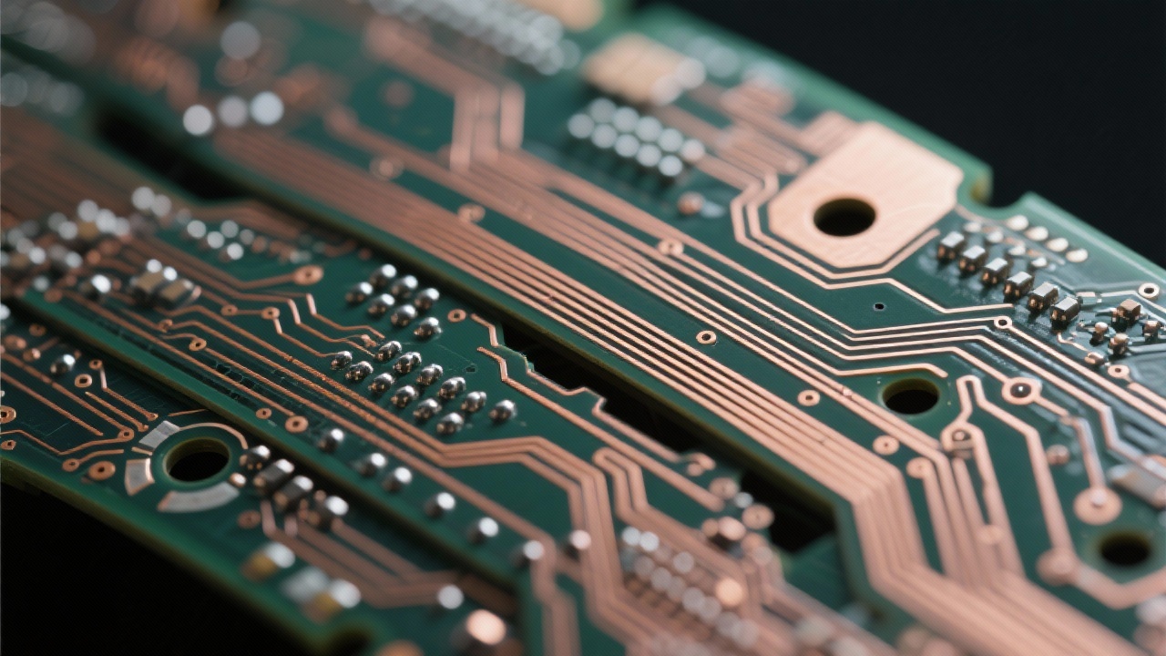
In the rapidly evolving landscape of semiconductor test equipment, the demand for high-density interconnect (HDI) PCBs has never been greater. As electronic devices continue to shrink while performance requirements escalate, PCB manufacturers face the daunting challenge of achieving precise control over 0.1mm laser microvias and 0.5mm back drilling processes simultaneously. This article explores the intricate balance required between these two critical technologies and provides actionable insights for overcoming common manufacturing hurdles.
Industry Insight:
According to recent market research, the global HDI PCB market is projected to grow at a CAGR of 8.7% from 2023 to 2028, driven primarily by demand from semiconductor test equipment and 5G infrastructure sectors. The ability to reliably produce boards with 0.1mm microvias and sub-0.5mm back drilling has become a key differentiator for manufacturers serving these high-tech industries.
The successful integration of microvia and back drilling technologies begins with a well-orchestrated process flow. The sequence starts with laser drilling of 0.1mm blind vias, followed by desmear and electroless copper deposition. After layer lamination, mechanical drilling creates the 0.5mm back drill holes, which are precisely aligned with the underlying microvias. This coordination requires meticulous planning to ensure that each process step complements rather than compromises the next.
Critical to this process is the management of stack-up tolerances. Each layer must maintain a thickness variation of less than ±5μm to ensure proper alignment between microvias and back drill holes. This level of precision demands advanced process control and real-time monitoring throughout the manufacturing sequence.
Addressing these challenges requires a multi-faceted approach. For instance, to control drill misalignment, advanced vision systems with sub-micron resolution are employed to ensure positional accuracy within ±3μm. Plating uniformity is achieved through pulse plating technology combined with agitation systems that maintain consistent electrolyte flow around microvias, resulting in thickness variation below 12%.
German-engineered precision equipment has proven instrumental in achieving the tight tolerances required for advanced HDI manufacturing. Laser drilling systems with nanosecond pulse technology can achieve hole positional accuracy of ±2μm at 3σ, while maintaining consistent hole diameter within ±3μm across the entire panel. Back drilling machines equipped with automatic tool length compensation and in-process measurement systems ensure that drill depth is controlled within ±5μm, critical for avoiding stub formation that degrades high-frequency performance.
The choice of substrate material significantly impacts microvia formation and reliability. Rogers materials, particularly those in the RO4000 series, offer superior dimensional stability with a coefficient of thermal expansion (CTE) of 6-8 ppm/°C in the z-axis, compared to 14-18 ppm/°C for standard FR-4. This reduced expansion minimizes layer separation during thermal cycling, a critical advantage for semiconductor test equipment operating in varying temperature environments.
However, Rogers materials come with a 30-40% cost premium over FR-4. For applications where cost sensitivity is a primary concern, high-performance FR-4 variants with modified resin systems can provide a viable alternative, offering CTE values as low as 10-12 ppm/°C while maintaining 70-80% of the performance characteristics of Rogers materials.
Implementing a closed-loop process control system has proven transformative for maintaining consistent quality in HDI manufacturing. By continuously monitoring key parameters such as drill feed rate, laser power, plating current density, and lamination pressure/temperature, manufacturers can make real-time adjustments to compensate for variables that affect microvia and back drill quality.
For example, when copper thickness variation exceeds 10%, the system automatically adjusts lamination pressure by ±5% and temperature by ±2°C to ensure proper resin flow and adhesion. This dynamic adjustment capability has been shown to reduce process variability by up to 40% and increase first-pass yield by an average of 15% in high-volume production environments.
Meeting IPC-III standards requires more than just occasional testing; it demands integrated quality control throughout the manufacturing process. For microvia reliability, this means implementing 100% automated optical inspection (AOI) with 2μm resolution to detect any anomalies in hole geometry or plating quality. Cross-section analysis, performed on a statistical basis of one panel per production run, verifies that microvia aspect ratios and plating thickness meet the stringent IPC-III requirements.
Thermal cycling testing, conducted on representative samples from each production lot, ensures that the HDI boards can withstand the 1,000 cycles from -40°C to +125°C required for semiconductor test equipment applications. This rigorous testing regime has resulted in field failure rates below 50 parts per million, well exceeding the industry average of 150 ppm for comparable HDI products.
Our team of engineering experts specializes in developing customized HDI solutions that overcome the most challenging manufacturing hurdles. Whether you're producing semiconductor test equipment or other high-performance electronics, we can help you achieve consistent quality and reliability.
Get Your Custom HDI PCB SolutionAs the semiconductor industry continues to push the boundaries of performance, the ability to reliably manufacture HDI PCBs with 0.1mm microvias and 0.5mm back drilling will remain a critical competitive advantage. By implementing the process controls, equipment capabilities, and material selection strategies discussed here, manufacturers can position themselves at the forefront of this rapidly evolving market segment.
 349
|
349
|
 double layer pcb rapid manufacturing
flying probe test
surface finish for pcb
pcb production process
quick prototype pcb
419
|
FPC high-density routing
flexible PCB design techniques
EMI optimization
signal crosstalk mitigation
flexible PCB manufacturing process
232
|
HDI PCB warpage control
IPC-II standard
semiconductor test PCB
multi-layer PCB design
PCB manufacturing precision
412
|
double layer PCB rapid manufacturing
PCB surface finishing technologies
flying probe testing
PCB production process
electrical reliability testing
298
|
FPC high - density wiring
Flexible circuit board design skills
Electromagnetic compatibility optimization
Signal crosstalk protection
High - reliability FPC manufacturing
double layer pcb rapid manufacturing
flying probe test
surface finish for pcb
pcb production process
quick prototype pcb
419
|
FPC high-density routing
flexible PCB design techniques
EMI optimization
signal crosstalk mitigation
flexible PCB manufacturing process
232
|
HDI PCB warpage control
IPC-II standard
semiconductor test PCB
multi-layer PCB design
PCB manufacturing precision
412
|
double layer PCB rapid manufacturing
PCB surface finishing technologies
flying probe testing
PCB production process
electrical reliability testing
298
|
FPC high - density wiring
Flexible circuit board design skills
Electromagnetic compatibility optimization
Signal crosstalk protection
High - reliability FPC manufacturing


-4.png?x-oss-process=image/resize,m_fill,h_800,w_800/format,webp)
-L4-4.png?x-oss-process=image/resize,m_fill,h_800,w_800/format,webp)


