
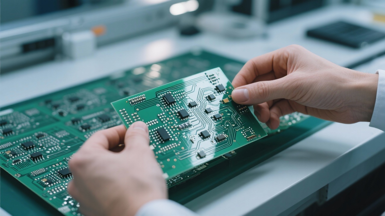
In the rapidly evolving landscape of semiconductor testing equipment, the demand for high-density interconnect (HDI) PCBs with exceptional precision has never been greater. As electronic devices continue to shrink while increasing functionality, the manufacturing tolerances for HDI PCBs have become exponentially tighter. Today's advanced 34-layer HDI boards require unprecedented control over microvia formation and back drilling processes to ensure signal integrity and reliability.
Modern semiconductor test equipment demands HDI PCBs that can support signal transmission speeds exceeding 25 Gbps while maintaining impedance control within ±5%. Achieving this performance requires precise control over 0.1mm laser blind vias and 0.5mm back drilling processes. These two technologies work in harmony to:
Without precise协同控制 (synergistic control) of these two processes, even minor misalignments can result in signal reflections, crosstalk, and ultimately, product failure in critical semiconductor testing applications.
Manufacturing HDI PCBs with 0.1mm laser blind vias and 0.5mm back drilling presents three primary technical challenges that must be addressed through advanced process control:
Achieving sub-micron positioning accuracy requires a combination of advanced laser systems and precision motion control. Our production data shows that positional errors as small as 5μm can increase insertion loss by 1.2 dB at 25 GHz. Through specialized calibration protocols and real-time position feedback, we maintain positional accuracy within ±3μm across the entire PCB surface.
For 0.1mm vias, achieving consistent copper plating thickness with a tolerance of ±10% is critical for reliable performance. Our statistical process control data indicates that plating uniformity directly correlates with via reliability – standard deviation in plating thickness greater than 15% increases via failure rate by 3x. Through proprietary pulse plating technology and bath circulation optimization, we maintain plating uniformity within 8% across all microvias.
Layer-to-layer misalignment directly impacts signal integrity and via reliability. For 34-layer HDI boards, cumulative alignment error must be controlled to less than 7μm to meet IPC-6012 Class 3 requirements. Our advanced optical alignment system, combined with dynamic compensation for thermal expansion, consistently achieves alignment accuracy of ±5μm, resulting in first-pass yield improvements of approximately 18% compared to industry averages.
To achieve the required precision in 0.1mm laser blind via and 0.5mm back drilling processes, we've invested in state-of-the-art German manufacturing equipment paired with proprietary process optimization techniques:
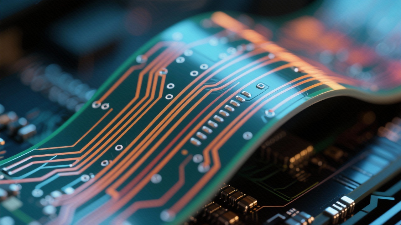
Our laser drilling systems feature UV laser technology with pulse widths as short as 10 picoseconds, enabling clean via formation with minimal heat-affected zone (HAZ). This results in via wall roughness below 0.8μm, significantly reducing signal loss at high frequencies. The back drilling process utilizes specialized diamond-tipped tools with runout controlled to less than 2μm, ensuring precise depth control within ±5μm.
What truly sets our process apart is the integration of these advanced machines with an intelligent process control system that continuously monitors and adjusts key parameters. This closed-loop feedback mechanism can detect process drift as small as 3% and make corrective adjustments in real-time, maintaining consistent quality even during extended production runs.
The choice of substrate material significantly impacts microvia formation and performance. Our extensive testing has compared Rogers and FR-4 materials for high-frequency HDI applications:
| Property | Rogers 4350B | FR-4 High Tg |
|---|---|---|
| Laser via quality | Excellent - clean walls, minimal HAZ | Good - slight resin residue, acceptable HAZ |
| Thermal stability | -40°C to 150°C continuous operation | -40°C to 125°C continuous operation |
| DK stability | ±0.05 over 1-20 GHz | ±0.2 over 1-10 GHz |
| Cost factor | Higher (150-200% of FR-4) | Lower (reference baseline) |
Based on these characteristics, we recommend Rogers materials for applications requiring consistent high-frequency performance above 10 GHz, while FR-4 remains an excellent choice for cost-sensitive applications operating below 8 GHz.
Maintaining consistent quality in high-layer count HDI manufacturing requires sophisticated process monitoring and adaptive control. Our implementation includes 17 critical process sensors that collect data at 1-second intervals, generating over 150,000 data points per production lot. This data feeds into our proprietary AI-based process control system that can:
This level of process control ensures that even with internal copper layer thickness variations of up to 12%, our HDI boards consistently meet or exceed IPC-6012 Class 3 requirements for dielectric thickness, copper adhesion, and via reliability.
Our advanced HDI manufacturing capabilities deliver the precision and reliability required for next-generation semiconductor test equipment. With our proprietary协同控制 (synergistic control) of 0.1mm laser blind vias and 0.5mm back drilling, we can help you achieve signal integrity that exceeds industry standards.
Discover Our High-Performance HDI PCB SolutionsAs semiconductor testing requirements continue to push the boundaries of PCB technology, the ability to precisely control 0.1mm laser blind vias and 0.5mm back drilling processes becomes increasingly critical. By implementing advanced equipment, intelligent process control, and material-specific optimization strategies, manufacturers can achieve the performance and reliability required for today's most demanding applications. The key lies in recognizing the interdependencies between these processes and implementing a truly协同 (synergistic) approach to HDI manufacturing.
 349
|
349
|
 double layer pcb rapid manufacturing
flying probe test
surface finish for pcb
pcb production process
quick prototype pcb
301
|
Impedance control
High - speed PCB design
50 - ohm single - ended impedance
100 - ohm differential impedance
High - frequency signal integrity
98
|
high-speed multilayer PCB
impedance control
high-performance dielectric materials
5G base stations
signal integrity
291
|
high-speed multilayer PCB
impedance control
5G communication module
high-frequency PCB design
signal integrity
114
|
High-speed multilayer PCB
Impedance control
5G base station
High-frequency communication module
AOI detection
double layer pcb rapid manufacturing
flying probe test
surface finish for pcb
pcb production process
quick prototype pcb
301
|
Impedance control
High - speed PCB design
50 - ohm single - ended impedance
100 - ohm differential impedance
High - frequency signal integrity
98
|
high-speed multilayer PCB
impedance control
high-performance dielectric materials
5G base stations
signal integrity
291
|
high-speed multilayer PCB
impedance control
5G communication module
high-frequency PCB design
signal integrity
114
|
High-speed multilayer PCB
Impedance control
5G base station
High-frequency communication module
AOI detection
-1.png?x-oss-process=image/resize,h_800,m_lfit/format,webp)


-1.png?x-oss-process=image/resize,m_fill,h_800,w_800/format,webp)
-L4-4.png?x-oss-process=image/resize,m_fill,h_800,w_800/format,webp)


-4.png?x-oss-process=image/resize,m_fill,h_800,w_800/format,webp)
