High-End HDI PCB Manufacturing: Precision Control of 0.1 mm Laser Microvias and 0.5 mm Back Drilling
2026-02-16
Technical knowledge
This article explains the core process control methods behind high-end HDI PCBs used in semiconductor test equipment, focusing on the coordinated precision of 0.1 mm laser blind microvias and 0.5 mm back drilling. It breaks down the end-to-end workflow and highlights practical solutions to the most common failure mechanisms—via misregistration, uneven copper plating on via walls, and layer-to-layer alignment errors that can lead to open circuits. It also outlines how advanced German precision equipment supports sub-millimeter tolerance management, and compares the microvia forming behavior of Rogers materials versus standard FR-4 to support smarter material selection. A data-driven quality approach is presented, showing how real-time process monitoring feeds back into adaptive lamination pressure and temperature profiles to stabilize results even under copper thickness variation. Compliance targets are anchored to IPC Class 3 requirements, including a minimum via copper thickness of 25 μm, providing actionable guidance for design engineers, process developers, and supply-chain owners aiming to improve yield and long-term reliability.

High-End HDI PCB Process Breakdown: Achieving 0.10 mm Laser Blind Vias with 0.50 mm Back Drilling—Without Losing Yield
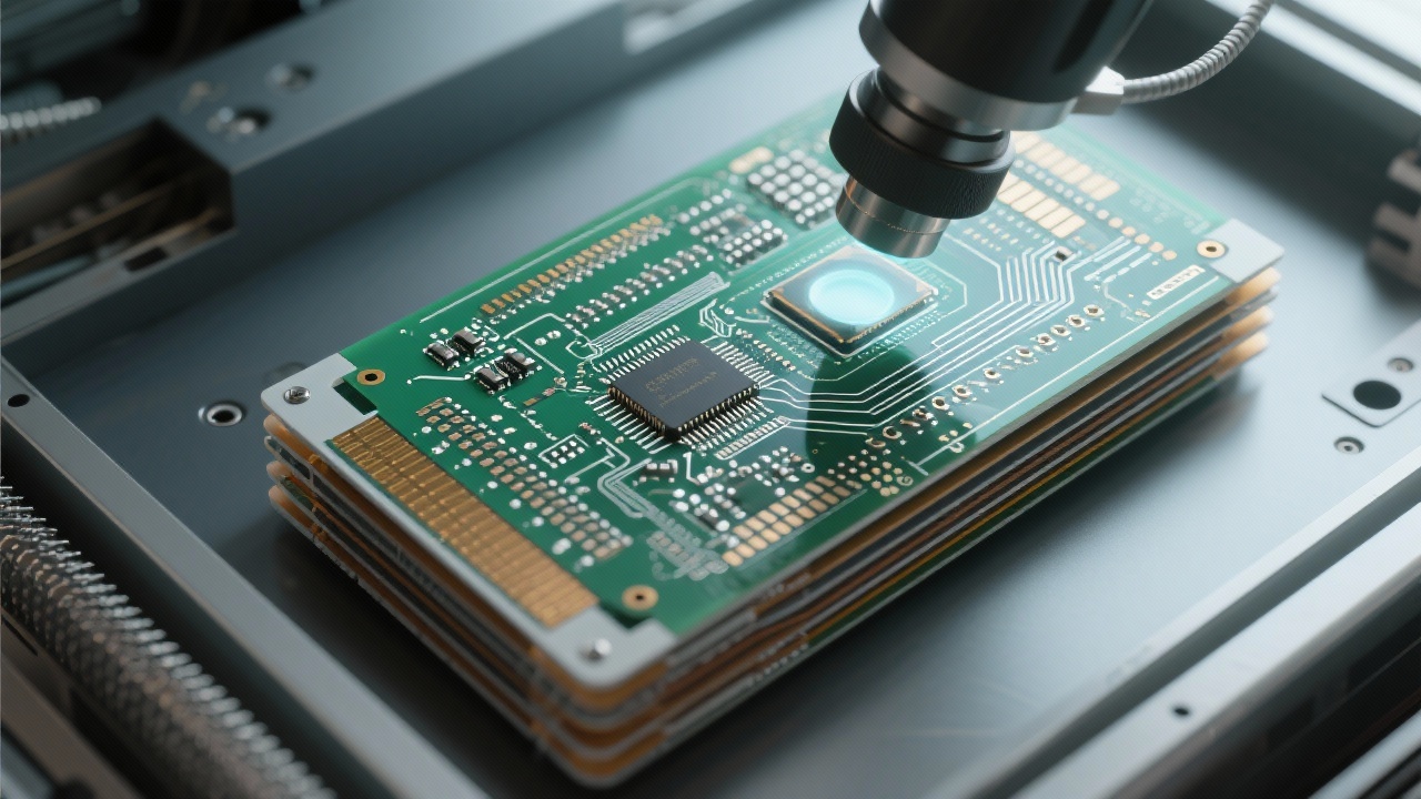
In semiconductor test equipment, an HDI PCB is rarely “just a board.” It is a precision interconnect platform where microvias, controlled impedance, and ultra-tight registration must behave consistently across volume builds. When 0.10 mm (100 μm) laser blind vias and 0.50 mm back drilling coexist in the same stack-up, the margin for process drift becomes extremely thin—especially under IPC Class 3 reliability expectations.
Below is a practical, engineering-first view of how leading manufacturers coordinate these two operations—covering drill-to-pad accuracy, plating uniformity, lamination-induced misregistration, and the data feedback loops that keep tolerances stable even when copper thickness varies.
1) Where the Real Challenge Starts: Microvia + Back Drill Interaction
On paper, laser drilling blind vias and mechanical back drilling target different features. In production, they “talk” through the stack-up: lamination flow, dielectric thickness tolerance, copper distribution, and layer-to-layer registration. A small shift in one stage can cascade into annular ring loss, stub residue, or plating weakness—each capable of triggering intermittent opens under thermal cycling.
Common tolerance targets used in high-end HDI builds (reference range):
• Laser blind via diameter: 0.10–0.12 mm
• Back drill diameter: 0.50–0.60 mm
• Drill-to-pad positional accuracy (critical nets): typically ±25 μm to ±50 μm
• Remaining stub after back drilling (high-speed test channels): often controlled to < 0.20 mm
• Board warpage for assembly stability: commonly kept at ≤ 0.50% (application dependent)
The most effective approach is not “optimize laser drilling” or “optimize back drilling” in isolation, but to build a coordinated control plan around the stack-up, the target registration budget, and the plating window.

2) Process Flow: The Key Nodes That Decide 0.10 mm / 0.50 mm Success
2.1 Registration Strategy Before Any Hole Is Made
High-end HDI lines treat registration as a designed system, not a last-minute CAM correction. Practical steps typically include: stable fiducial design, balanced copper distribution to reduce lamination distortion, and pre-defined scaling rules for inner layers. In builds where the back drill must stop cleanly near target pads, manufacturers often allocate a tighter registration budget to the drilled layers than to non-critical layers.
2.2 Laser Blind Via Formation (0.10 mm) That Plates Reliably
Laser parameters are tuned around dielectric ablation consistency and copper land integrity. A recurring reliability risk is not the via diameter itself, but the combination of taper angle, smear/residue, and micro-roughness that influences metallization continuity. For 0.10 mm blind vias, many Class 3-oriented processes aim for stable via profiles that support uniform copper deposition at the via knee, where stress concentrates.
2.3 Plating Window Control: Uniform Copper in Tiny Geometry
Microvia plating failures often show up as “random” opens, but the physics are systematic: current density gradients and solution exchange limitations worsen as features shrink. Manufacturers pursuing consistent Class 3 performance typically focus on: agitation and filtration stability, bath analytics cadence, and panel-level current distribution design. In many high-reliability HDI lines, the process is built to consistently reach a minimum hole copper thickness of ~25 μm on critical interconnects—without over-plating outer copper beyond what etching can hold.
2.4 Back Drilling (0.50 mm): Stop Depth Accuracy Beats Speed
Back drilling is frequently judged by diameter alone, but performance depends more on depth control and repeatability across the panel. For high-speed test interfaces, the objective is predictable stub length, because stub variation can introduce measurable reflections and degrade eye diagrams. Practical control methods include: calibrated depth tables per stack-up, frequent tool wear checks, and post-drill verification sampling (especially when resin content or dielectric thickness shifts lot-to-lot).
3) Failure Modes and How High-End Lines Reduce Them
3.1 Hole Offset and Annular Ring Loss
Offset is usually a combined outcome of imaging scale error, lamination movement, and drilling coordinate drift. In advanced HDI factories, corrective actions often include tighter inner-layer scaling control, controlled lamination press recipes, and inline coordinate compensation. When the blind via diameter is 0.10 mm, even a 40–60 μm shift can be the difference between a robust ring and a borderline ring—especially on dense BGA fanout.
3.2 Plating Non-Uniformity at the Via Knee
Microvias tend to concentrate stress where the via meets the capture pad. If copper builds unevenly, the thinnest region becomes the first crack initiation point during thermal cycling. Strong processes aim to keep microvia copper deposition stable panel-to-panel by enforcing consistent pretreatment, maintaining bath chemistry within narrow limits, and using real-time tracking of current density and temperature.
3.3 Layer Misregistration After Lamination
Misregistration is not always visible until back drilling exposes a tolerance stack issue: the drill may “chase” a nominal target that has moved. High-end HDI processes often reduce this by balancing copper, controlling prepreg flow, and using press recipes that stabilize z-axis thickness. For multi-lam builds, even small thickness deviations (for example, ±40 μm on dielectric) can materially shift stop-depth margins.
4) Why German Precision Equipment Matters (and What to Verify)
Equipment alone does not guarantee Class 3 yields, but high-end German platforms are widely chosen for one reason: repeatable motion control under tight thermal and mechanical drift constraints. In microvia + back drill combinations, the most valuable capabilities are stable coordinate accuracy, consistent spindle behavior, and robust vision alignment—not just headline speed.
Practical checklist for equipment-enabled tolerance control
- Vision-based alignment stability across long runs (not just first panel performance)
- Depth control repeatability for back drilling across panel positions and stack-up lots
- Tool wear monitoring cadence and drill bit life rules tied to Cp/Cpk trends
- Data logging that can be correlated to plating and lamination outcomes
5) Rogers vs FR-4 in Microvia Formation: What Changes in Real Production
Material selection is not purely an electrical decision; it is also a manufacturability decision. In microvia formation, different resin systems respond differently to laser energy, and different glass styles influence cleanliness and taper. For back drilling, thickness stability and resin behavior under lamination also determine how safely the drill can “stop” without leaving excessive stub or cutting into targets.
| Factor |
FR-4 (High-Tg / Low-loss variants) |
Rogers (typical RF laminates) |
| Laser drilling behavior |
Generally stable; glass/resin mix may increase debris risk if parameters drift |
Material-dependent; some systems require tighter laser tuning to avoid resin recession |
| Via wall condition |
Often robust with well-controlled desmear/etchback |
May need specialized surface prep to ensure strong metallization adhesion |
| Thickness stability (lamination) |
Predictable in mature recipes; still sensitive to copper balance |
Can be excellent, but process windows vary by laminate family and bonding system |
| Best-fit use case |
Dense digital + mixed-signal where cost and supply stability matter |
High-frequency paths where dielectric performance dominates, with tighter process governance |
For semiconductor test PCBs, many teams adopt a hybrid approach: RF laminates where signal integrity demands it, and robust FR-4 variants elsewhere—while enforcing a unified registration and plating control plan so the manufacturing risk does not fragment across materials.

6) Data-Driven Process Control: How Good Lines Stay Stable When Copper Thickness Drifts
The most repeatable HDI programs treat manufacturing as a closed loop: drill results inform plating settings, lamination thickness trends adjust back drill depth recipes, and electrical test/inspection outcomes trigger parameter refinement. Instead of waiting for end-of-line failures, they watch “early indicators.”
Typical early indicators used to protect yield
- Microvia diameter drift beyond ~±10 μm trend line triggers laser parameter review
- Panel thickness trend shift beyond ~±30–50 μm prompts lamination recipe adjustment
- Plating thickness distribution widening (higher σ) triggers bath and current distribution checks
- Back drill depth Cp/Cpk dropping below typical control targets (e.g., ≥1.33) prompts recalibration and tool review
A subtle but important benefit of this feedback approach is that it can compensate for normal copper thickness variation (for example, outer layer copper shifting by several microns across lots) without forcing unnecessary design changes or over-tightening incoming inspection to impractical levels.
7) IPC Class 2 vs Class 3: The Reliability Bar That Shapes the Process
Many semiconductor test applications align closer to IPC Class 3 expectations because intermittent failures are far more expensive than initial fabrication cost. This directly impacts microvia and back drill controls: more robust copper in holes, tighter registration governance, and stricter acceptance criteria for defects that could propagate under vibration and thermal shock.
IPC reference note (for buyer alignment): IPC Class 2 generally targets “dedicated service electronic products,” while IPC Class 3 targets “high reliability electronic products.” In practice, Class 3 programs often require tighter control of plating integrity and defect allowances. For high-end HDI interconnects, a commonly used manufacturing target is ≥ 25 μm minimum copper thickness in holes on critical structures, subject to the applicable IPC specification and customer drawing notes.
Ready to De-Risk Your Next HDI Build?
If your design includes 0.10 mm laser blind vias, 0.50 mm back drilling, IPC Class 3 expectations, or mixed materials (Rogers + FR-4), the fastest way to protect yield is to review the stack-up and control plan together—before release.
Share your stack-up, target via structure, and back drill depth requirements to receive a manufacturability-focused response.


-1.png?x-oss-process=image/resize,m_fill,h_800,w_800/format,webp)
-4.png?x-oss-process=image/resize,m_fill,h_800,w_800/format,webp)


-4.png?x-oss-process=image/resize,h_800,m_lfit/format,webp)


