
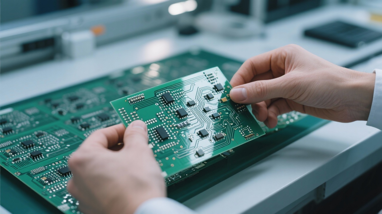
In today’s high-speed electronics landscape—driven by 5G infrastructure, AI servers, and advanced RF systems—the demand for reliable, high-density printed circuit boards (PCBs) has never been higher. At Ruiheng PCB, we’ve engineered a 24-layer high-frequency PCB solution featuring 3mil trace width technology, delivering measurable improvements in signal integrity, thermal management, and manufacturability.
Traditionally, PCB designers faced a trade-off between routing density and signal loss. But with our 3mil (0.076mm) trace capability—validated through rigorous IPC-6012 Class 3 testing—we achieve both. According to internal process validation data, this precision allows up to 25% more traces per layer compared to standard 5mil designs, while reducing insertion loss by an average of 12–18% at frequencies above 10 GHz.
This is made possible through advanced photolithography and controlled-depth etching processes that maintain consistent copper thickness across all layers. Our automated optical inspection (AOI) system ensures 99.7% trace accuracy, minimizing defects like necking or bridging—critical for microwave and millimeter-wave applications.
Our clients in the telecom and aerospace sectors have successfully deployed these boards in:
These results aren’t just theoretical—they’re backed by real-world test reports from Tier-1 customers who now rely on Ruiheng PCBs for mission-critical products.
If your project involves high-frequency signals (>6GHz), dense component placement, or strict EMI requirements, a 24-layer board with 3mil lines isn’t just an option—it’s a necessity. The improved layer-to-layer alignment, tighter impedance control (<±5%), and enhanced via reliability reduce design iterations by up to 40%, saving time and cost during prototyping.
And because we build with RoHS-compliant materials and support full DFM (Design for Manufacturability) reviews upfront, you can focus on innovation—not manufacturing headaches.
 220
|
220
|
 FPC high - density routing
Flexible circuit board design techniques
Electromagnetic compatibility optimization
High - density routing solutions
Flexible PCB manufacturing processes
427
|
yellow coverlay for FPC
EMI shielding in flexible circuits
PI FR-4 composite substrate
high-frequency signal integrity
FPC manufacturing process
146
|
high-speed multilayer PCB impedance control
50 ohm single-ended impedance
100 ohm differential impedance
high-frequency PCB design
signal integrity optimization
227
|
high-precision FPC design
2mil trace width
4-layer flexible PCB
ENIG surface finish
impedance control
183
|
high-frequency multilayer PCB
impedance control technology
5G base station PCB design
high-speed telecom PCB
AOI inspection
FPC high - density routing
Flexible circuit board design techniques
Electromagnetic compatibility optimization
High - density routing solutions
Flexible PCB manufacturing processes
427
|
yellow coverlay for FPC
EMI shielding in flexible circuits
PI FR-4 composite substrate
high-frequency signal integrity
FPC manufacturing process
146
|
high-speed multilayer PCB impedance control
50 ohm single-ended impedance
100 ohm differential impedance
high-frequency PCB design
signal integrity optimization
227
|
high-precision FPC design
2mil trace width
4-layer flexible PCB
ENIG surface finish
impedance control
183
|
high-frequency multilayer PCB
impedance control technology
5G base station PCB design
high-speed telecom PCB
AOI inspection


-L4-4.png?x-oss-process=image/resize,m_fill,h_800,w_800/format,webp)


-4.png?x-oss-process=image/resize,m_fill,h_800,w_800/format,webp)
-1.png?x-oss-process=image/resize,m_fill,h_800,w_800/format,webp)


