
In modern telecommunications, particularly in high-speed 5G base stations and high-frequency communication modules, precise impedance control in multi-layer printed circuit boards (PCBs) is paramount to ensuring signal integrity and minimizing loss. This article delves into the core principles and real-world applications of impedance control in high-frequency, multi-layer PCB design, focusing on the widely adopted single-ended 50Ω and differential 100Ω impedance standards. Through a technical yet accessible approach, it explores how advanced dielectric materials, meticulous manufacturing tolerances, and state-of-the-art testing methods converge to enable industry-leading PCB solutions that underpin next-generation communication technologies.
Signal integrity in high-frequency circuit boards hinges critically on maintaining controlled impedance along transmission lines. The industry standard often stipulates 50 ohms for single-ended traces and 100 ohms for differential pairs, which are essential for balanced signal propagation and noise rejection. Mismatches in these impedances can cause signal reflections, increased insertion loss, and crosstalk, degrading system performance especially at frequencies beyond several gigahertz.
Designing for optimal impedance requires combined efforts in layout geometry, material selection, and stack-up configuration. For example, 5G base station PCBs frequently employ microstrip and stripline structures optimized through electromagnetic simulation tools that model trace width, spacing, and dielectric thickness to achieve targeted impedance values. Differential signaling, ubiquitous in high-speed data lines, utilizes pair spacing and symmetry to reach 100Ω differential impedance, improving noise immunity crucial for stable high-frequency transmission.
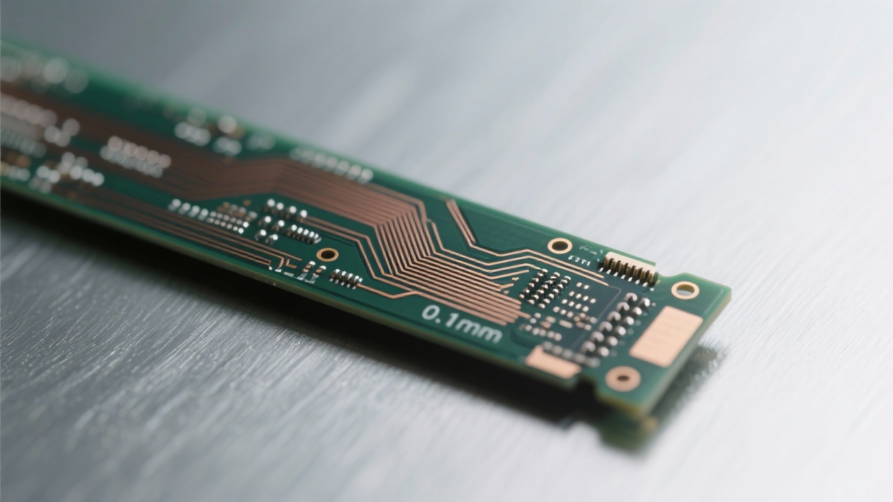
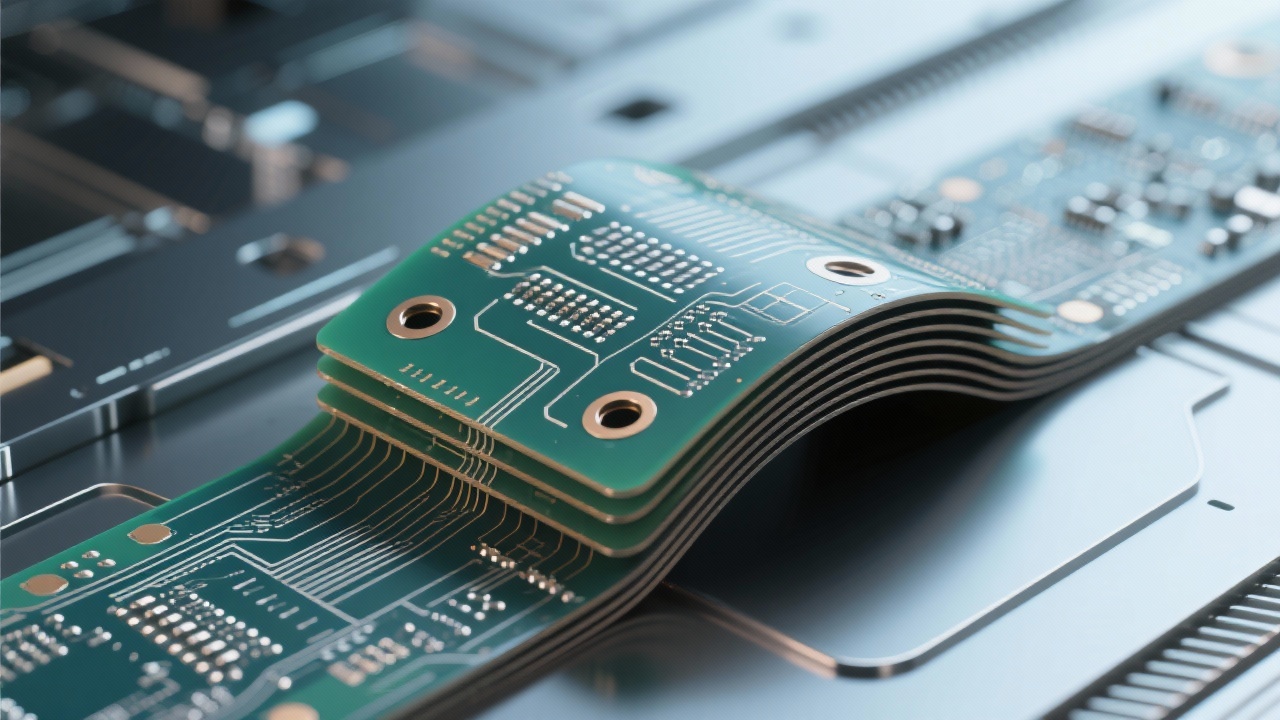
The choice of dielectric substrates directly impacts signal velocity and attenuation. High-performance materials such as Rogers RO4350B or low-loss prepregs are favored for their stable dielectric constants (Dk) and low dissipation factors (Df), ensuring impedance stability over temperature and frequency variations. Manufacturing precision, particularly in layer lamination and copper foil thickness, is tightly controlled within micron-level tolerances to avoid impedance shifts that can exceed ±3%, which is vital when working with dense 24-layer high-frequency PCB stacks.
Verifying impedance accuracy throughout production demands precise testing methods. Time Domain Reflectometry (TDR) and Vector Network Analyzer (VNA) measurements provide detailed reflection coefficient data to detect impedance mismatches. Automated Optical Inspection (AOI) supplemented by optical microscopy enables detection of micro-fabrication defects that may affect impedance continuity. Employing these combined techniques throughout the fabrication process enhances yield and consistency essential for telecommunications equipment reliability.
Our latest 24-layer, high-frequency PCB offerings integrate cutting-edge materials and refined manufacturing processes tailored for demanding telecom applications. Key advantages include superior impedance stability within ±3%, minimal insertion loss optimized for multi-gigabit data rates, and robust electromagnetic compatibility. These solutions excel in complex 5G base station modules and high-speed communication boards, delivering consistent performance in real-world deployments where precise impedance translates into enhanced data throughput and signal reliability.
 402
|
402
|
 FPC high-density routing
flexible circuit board design tips
EMC optimization
high-density PCB trace spacing
flexible printed circuit manufacturing
360
|
High-density FPC routing
Flexible circuit board design
Electromagnetic compatibility optimization
Precision FPC manufacturing
Flexible PCB reliability
256
|
multilayer flexible pcb via design
high-density fpc routing
fpc electromagnetic compatibility
flexible circuit board manufacturing capability
fpc bend zone reliability
317
|
high-density FPC routing
flexible PCB design
EMI optimization
medical FPC
consumer electronics FPC
156
|
multilayer flexible pcb via design
micro-hole processing in fpc
high-density flex pcb layout
emc optimization in flexible circuits
flexible pcb manufacturing process
FPC high-density routing
flexible circuit board design tips
EMC optimization
high-density PCB trace spacing
flexible printed circuit manufacturing
360
|
High-density FPC routing
Flexible circuit board design
Electromagnetic compatibility optimization
Precision FPC manufacturing
Flexible PCB reliability
256
|
multilayer flexible pcb via design
high-density fpc routing
fpc electromagnetic compatibility
flexible circuit board manufacturing capability
fpc bend zone reliability
317
|
high-density FPC routing
flexible PCB design
EMI optimization
medical FPC
consumer electronics FPC
156
|
multilayer flexible pcb via design
micro-hole processing in fpc
high-density flex pcb layout
emc optimization in flexible circuits
flexible pcb manufacturing process


-1.png?x-oss-process=image/resize,m_fill,h_800,w_800/format,webp)

-4.png?x-oss-process=image/resize,m_fill,h_800,w_800/format,webp)