
In the realm of high-speed multilayer PCB design, impedance control stands as a cornerstone for ensuring signal integrity. The standard impedance values of 50 ohms for single-ended and 100 ohms for differential pairs play a pivotal role in signal transmission. Research shows that maintaining these impedance standards can reduce signal reflection by up to 80%, significantly enhancing the overall performance of 5G communication devices.
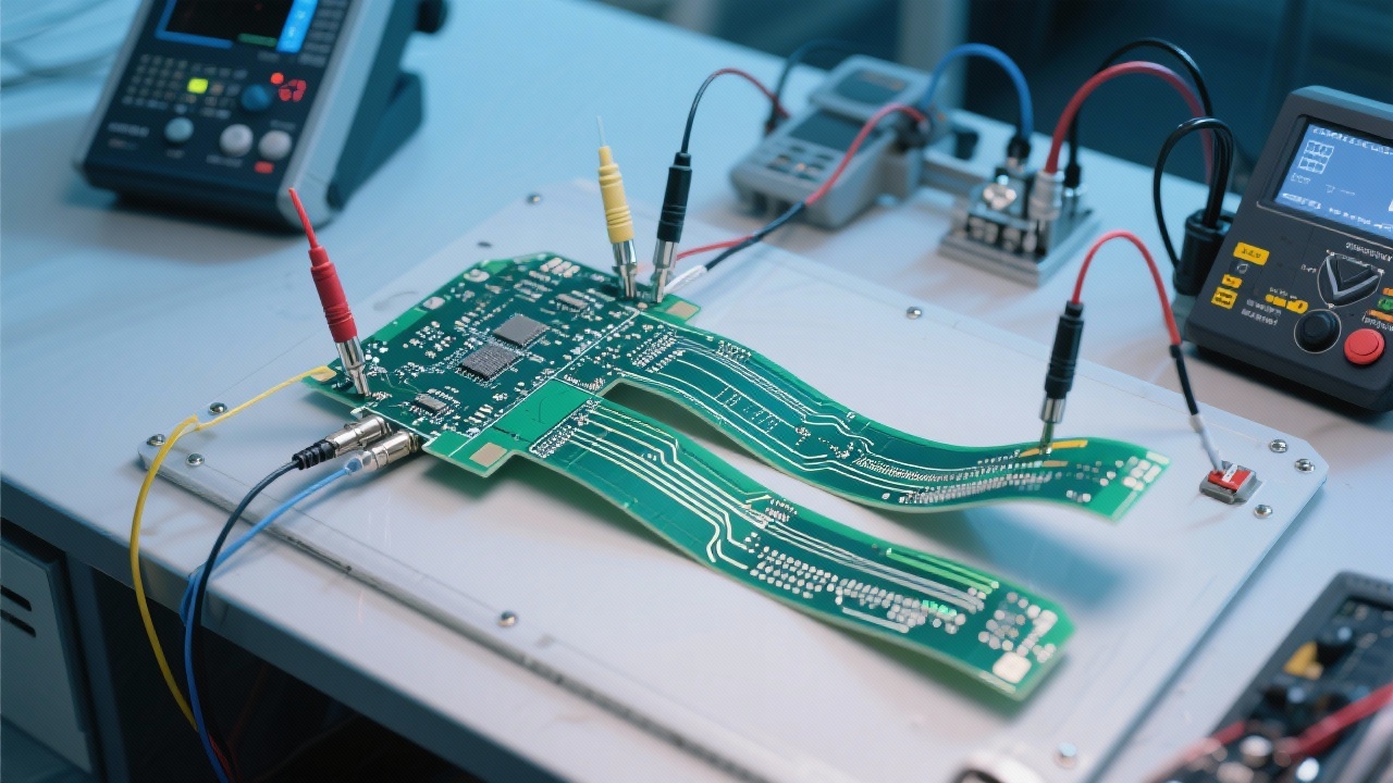
When the impedance is not properly controlled, signal distortion can occur, leading to issues such as data loss and reduced communication efficiency. For instance, in a 5G base station, improper impedance can cause interference in the high-frequency signals, affecting the coverage and quality of the network.
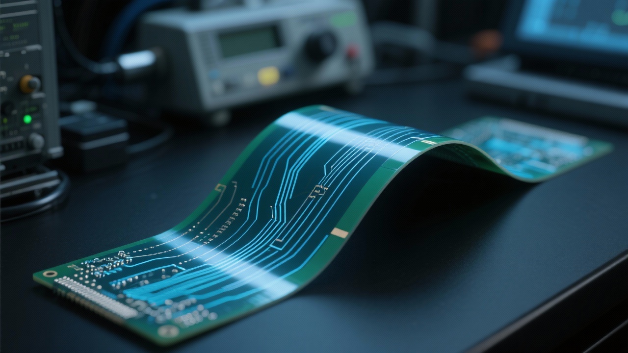
Impedance matching is a crucial technique in high-speed PCB design. By carefully selecting the right materials and design methods, engineers can achieve optimal impedance matching. In 5G base stations and high-frequency communication modules, impedance matching techniques are widely applied to ensure stable signal transmission.
Take a 5G base station project as an example. Through precise impedance matching design, the signal loss in the high-frequency communication module was reduced by 30%, greatly improving the overall performance of the base station. The design methods involve adjusting the width and spacing of the traces, as well as the thickness of the dielectric layer.
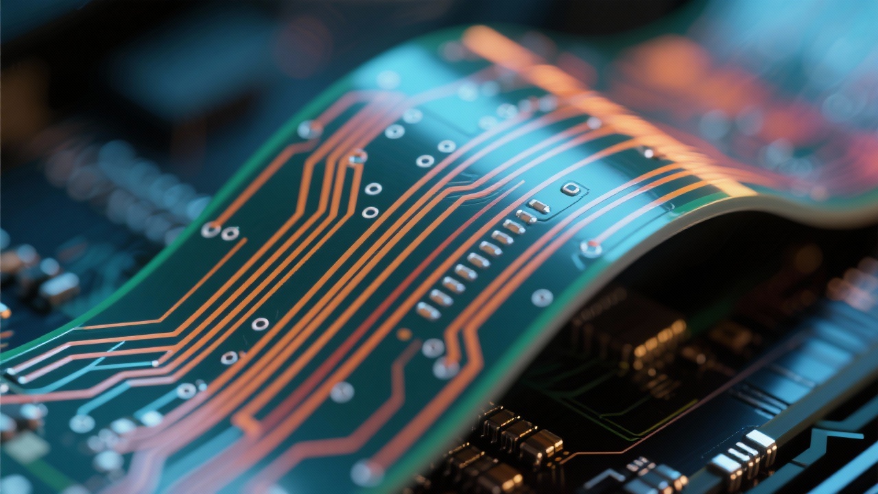
High-performance materials and strict manufacturing tolerances are essential for maintaining impedance stability. The characteristics of the dielectric materials, such as dielectric constant and loss tangent, have a significant impact on impedance. By using materials with low loss and stable dielectric constants, engineers can reduce signal reflection and crosstalk.
In addition, strict manufacturing tolerances are required to ensure the consistency of the impedance. For example, the tolerance of the trace width should be controlled within ±0.05mm to ensure the accuracy of the impedance. This can effectively reduce signal distortion and improve the reliability of the 5G communication devices.
To ensure the quality of the high-speed multilayer PCBs, advanced impedance measurement and verification technologies are necessary. Design simulation and automatic optical inspection (AOI) are two important methods.
Design simulation allows engineers to predict the impedance performance of the PCB before manufacturing. By adjusting the design parameters in the simulation, the impedance can be optimized. AOI detection can quickly and accurately detect any defects in the PCB, ensuring that the impedance meets the design requirements. These technologies can significantly improve the product quality and reduce the production cost.
Are you looking for a leading high-speed multilayer PCB manufacturing solution to enhance the performance of your 5G communication devices? Click here to learn more.
 419
|
419
|
 Flexible Leiterplatte Design
Signalinterferenz vermeiden
EMV Optimierung FPC
Hochdichte FPC-Bestückung
FPC Herstellungstechnologie
315
|
Hochgeschwindigkeits-Mehrlagen-PCB
Impedanzkontrolltechnik
AOI-Prüfung
Signalintegrität
5G-Kommunikations-PCB
430
|
high-speed multilayer pcb impedance control
50 ohm single ended impedance
100 ohm differential impedance
rf pcb design
signal integrity optimization
298
|
Hochdichte Verdrahtung von FPCs
Designtechniken für flexible Leiterplatten
Optimierung der elektromagnetischen Verträglichkeit
Schutz gegen Signalkreuzstörungen
Herstellung von FPCs mit hoher Zuverlässigkeit
447
|
Hochdichte Verdrahtung von FPC
Entwurfstechniken für flexible Leiterplatten
Optimierung der elektromagnetischen Verträglichkeit
Hochdichte flexible PCB
Via - Entwurfstandards
Flexible Leiterplatte Design
Signalinterferenz vermeiden
EMV Optimierung FPC
Hochdichte FPC-Bestückung
FPC Herstellungstechnologie
315
|
Hochgeschwindigkeits-Mehrlagen-PCB
Impedanzkontrolltechnik
AOI-Prüfung
Signalintegrität
5G-Kommunikations-PCB
430
|
high-speed multilayer pcb impedance control
50 ohm single ended impedance
100 ohm differential impedance
rf pcb design
signal integrity optimization
298
|
Hochdichte Verdrahtung von FPCs
Designtechniken für flexible Leiterplatten
Optimierung der elektromagnetischen Verträglichkeit
Schutz gegen Signalkreuzstörungen
Herstellung von FPCs mit hoher Zuverlässigkeit
447
|
Hochdichte Verdrahtung von FPC
Entwurfstechniken für flexible Leiterplatten
Optimierung der elektromagnetischen Verträglichkeit
Hochdichte flexible PCB
Via - Entwurfstandards


-L4-4.png?x-oss-process=image/resize,m_fill,h_800,w_800/format,webp)

-1.png?x-oss-process=image/resize,m_fill,h_800,w_800/format,webp)
