
In the rapidly evolving landscape of 5G and high-frequency communication systems, precise impedance control is paramount to maintaining signal integrity. This guide explores the fundamental principles behind industry-standard impedance values—50Ω single-ended and 100Ω differential—and illustrates how advanced materials such as ISOLA 370HR and MENTRON6, combined with rigorous manufacturing tolerance management and Automated Optical Inspection (AOI) technology, ensure reliable and high-performance multilayer PCB production.
Impedance reflects the opposition a circuit presents to the flow of high-frequency current, combining resistive, inductive, and capacitive effects. Maintaining a precise 50Ω single-ended or 100Ω differential impedance ensures minimal signal reflection and crosstalk, which are major sources of data errors and reduced transmission rates in high-speed digital circuits. The choice of these impedance benchmarks is based on extensive industry consensus and empirical validation in RF and data communications.
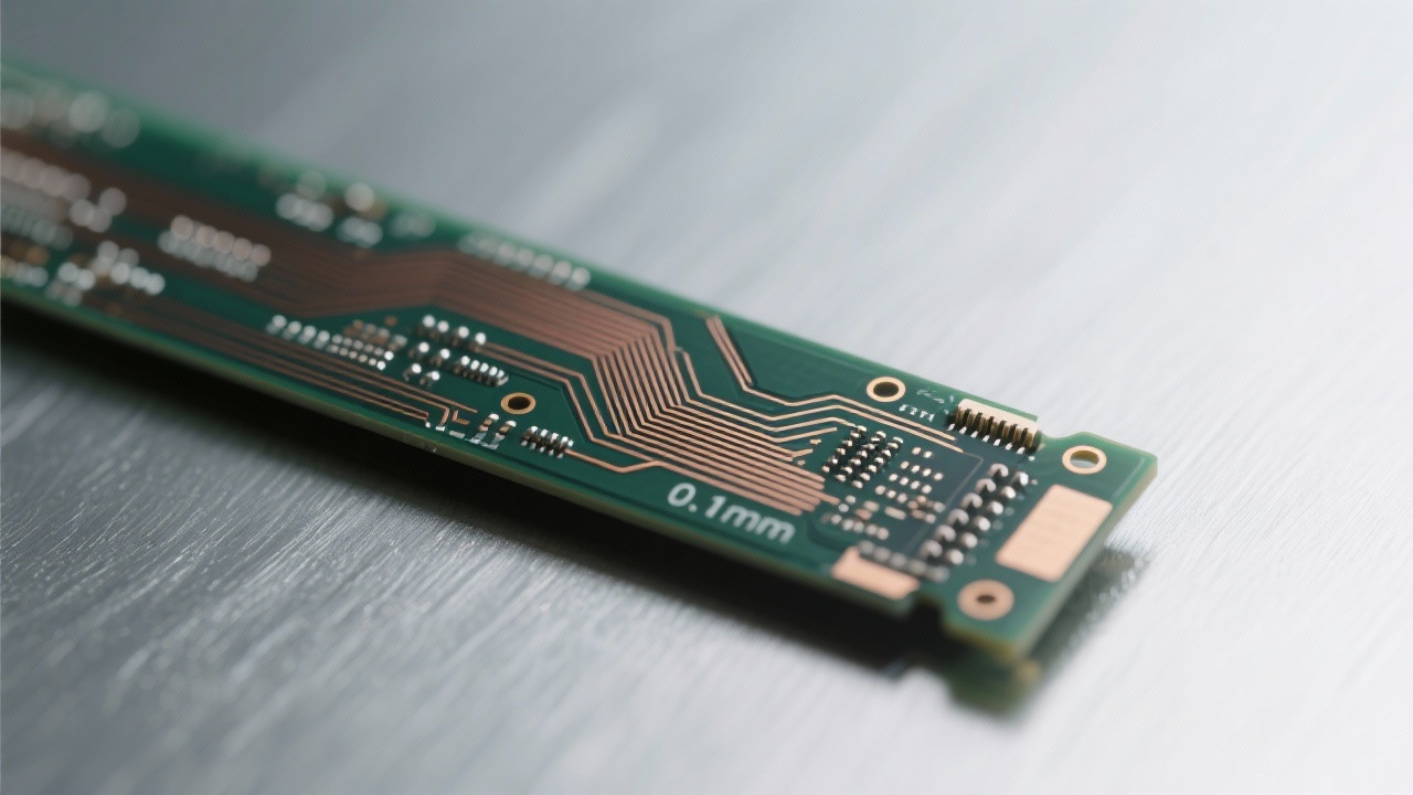
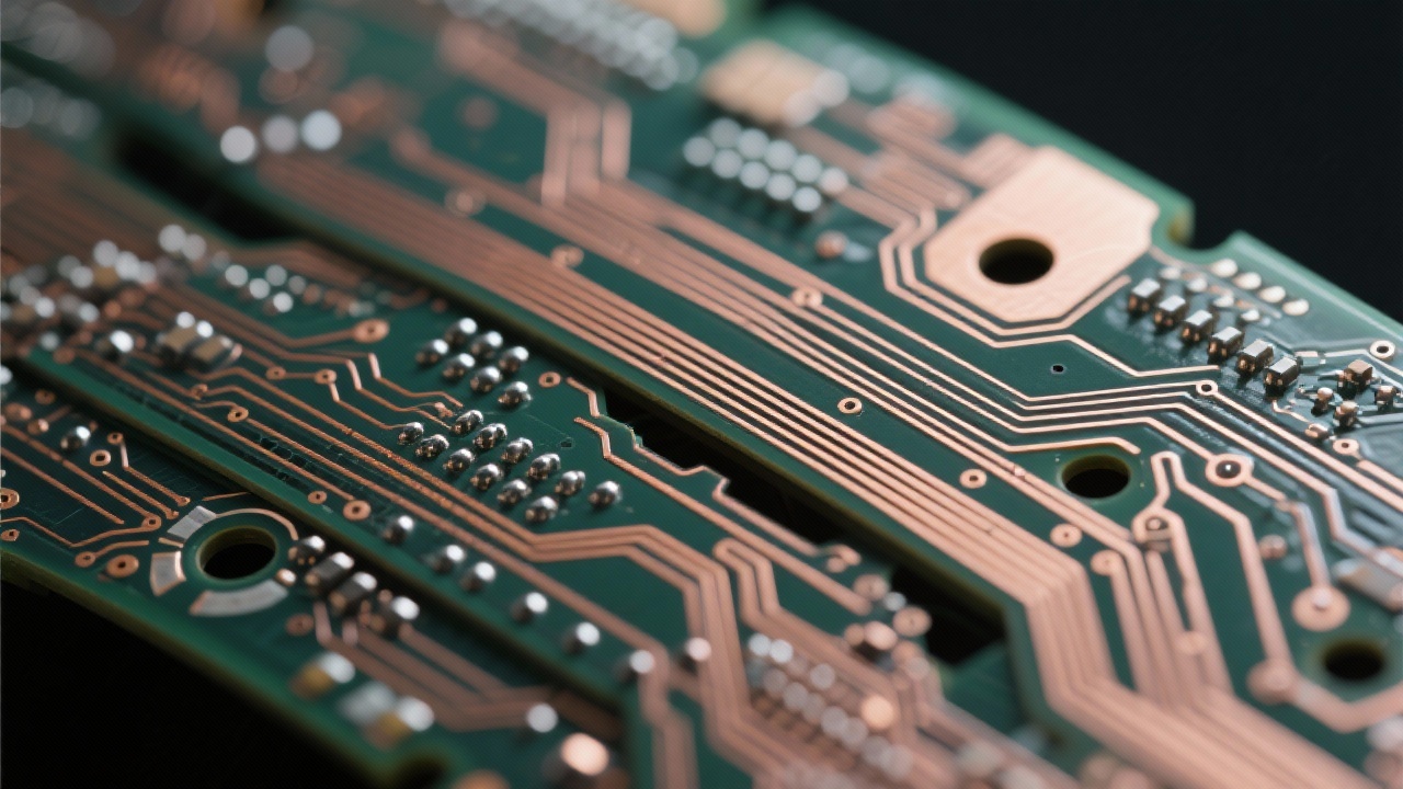
In real-world manufacturing, achieving stable impedance requires meticulous stack-up design and tight control over critical parameters such as dielectric thickness, conductor width, and spacing. For 5G base station modules, impedance mismatches can cause signal degradation, manifesting as increased bit error rates or compromised throughput.” By implementing precision lamination combined with 3-mil line width and spacing tolerances, manufacturers can sustain impedance variation within ±5%, a standard range accepted for high-frequency PCB reliability.
Signal integrity improvements from controlled impedance often translate to up to 30% reduction in reflection losses and a measurable decrease in crosstalk noise below -40 dB, which is critical to maintaining 5G network robustness.
High-performance dielectric materials like ISOLA 370HR and MENTRON6 play a crucial role in stabilizing impedance by offering low dissipation factors and consistent dielectric constants over a wide frequency range. These materials reduce dielectric losses and provide thermal and chemical resilience necessary for dense multilayer PCB assemblies used in telecom systems.
Collaborating closely with PCB fabricators to implement manufacturing processes with controlled variations in copper foil thickness, dielectric layer uniformity, and lamination pressure further minimizes impedance drift. Such coordinated material and process optimization ensure that impedance stays within target ranges despite environmental stressors.
AOI technology has become an indispensable tool in the quality assurance workflow, enabling rapid and non-destructive detection of short circuits, open circuits, and surface defects such as scratches or contaminations that can affect impedance consistency and board reliability. High-resolution imaging paired with advanced algorithms allows for 100% inspection in-line, reducing reliance on manual checks and preventing defective boards from progressing down the assembly line.
Integrating AOI with impedance measurement data creates a closed-loop system for proactive quality control, correlating defect detection with electrical parameter deviations to optimize process parameters continuously. This synergy enhances yield rates and lowers scrap costs, proving invaluable for complex multilayer PCBs in mission-critical telecom applications.
Consider a 5G base station PCB where both single-ended 50Ω and differential 100Ω impedances coexist within tight spatial constraints. Achieving impedance uniformity in such complex multilayer assemblies demands synchronized control over material properties, precise manufacturing tolerances, and comprehensive defect inspections. Implementing the described methods has demonstrated a significant reduction of signal reflections by 28% and crosstalk suppression improvements achieving levels better than -45 dB, directly translating into enhanced data throughput and system reliability.
For engineers and designers seeking deeper insights or practical resources, download our comprehensive impedance simulation models and AOI inspection report templates. These tools are tailored to accelerate your development cycle and strengthen quality assurance processes in high-speed PCB manufacturing.
 419
|
419
|
 Flexible Leiterplatte Design
Signalinterferenz vermeiden
EMV Optimierung FPC
Hochdichte FPC-Bestückung
FPC Herstellungstechnologie
220
|
FPC Hochdichte-Wirng
Flex-PCB-Design-Tipps
EMC-Optimierung
Hochdichte-Leitungsrouting-Lösungen
Flex-PCB-Fertigungstechnologie
291
|
Hochgeschwindigkeits-Multilayer-PCB
Impedanzkontrolle
5G-Kommunikationsmodul
Hochfrequenz-PCB-Design
AOI-Test
152
|
Impedanzkontrolle
5G-Basisstationen PCB
Hochfrequenzmodul
Hochgeschwindigkeitsmultilayer-PCB
Signalintegrität
216
|
Hochgeschwindigkeits-PCB-Impedanzkontrolle
5G-Basisstation-PCB-Design
Hochfrequenzkommunikationsmodul-Impedanzanpassung
Hochleistungs-Dielektrikamaterial-PCB
PCB-Signalintegrität
Flexible Leiterplatte Design
Signalinterferenz vermeiden
EMV Optimierung FPC
Hochdichte FPC-Bestückung
FPC Herstellungstechnologie
220
|
FPC Hochdichte-Wirng
Flex-PCB-Design-Tipps
EMC-Optimierung
Hochdichte-Leitungsrouting-Lösungen
Flex-PCB-Fertigungstechnologie
291
|
Hochgeschwindigkeits-Multilayer-PCB
Impedanzkontrolle
5G-Kommunikationsmodul
Hochfrequenz-PCB-Design
AOI-Test
152
|
Impedanzkontrolle
5G-Basisstationen PCB
Hochfrequenzmodul
Hochgeschwindigkeitsmultilayer-PCB
Signalintegrität
216
|
Hochgeschwindigkeits-PCB-Impedanzkontrolle
5G-Basisstation-PCB-Design
Hochfrequenzkommunikationsmodul-Impedanzanpassung
Hochleistungs-Dielektrikamaterial-PCB
PCB-Signalintegrität


-L4-4.png?x-oss-process=image/resize,m_fill,h_800,w_800/format,webp)


-1.png?x-oss-process=image/resize,h_800,m_lfit/format,webp)


