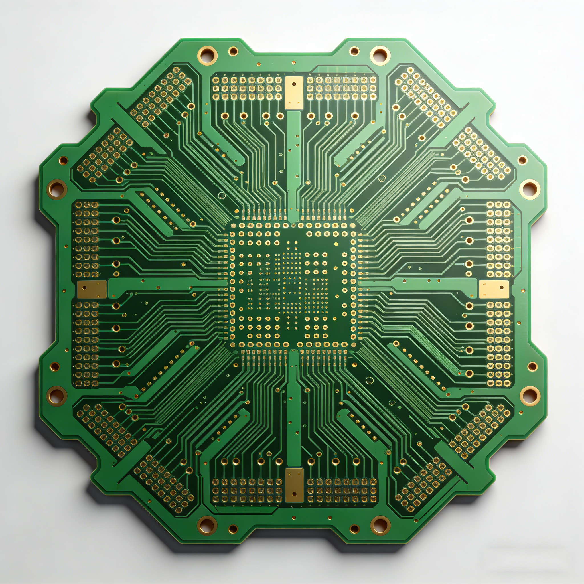
In today's rapidly evolving telecommunications landscape, 5G technology demands unprecedented data transmission speeds reaching 10 Gbps and beyond, with latency requirements dropping below 1 millisecond. As communication modules push frequency boundaries into the 24 GHz to 40 GHz millimeter-wave spectrum, printed circuit boards (PCBs) have transitioned from passive mechanical platforms to active participants in signal integrity management. This evolution has made precise impedance control not merely a technical specification but a fundamental requirement for reliable 5G system performance.
The telecommunications industry has established two primary impedance standards that serve as the foundation for reliable high-frequency signal transmission:
Widely adopted for radio frequency (RF) circuits and antenna connections, 50Ω impedance represents the optimal balance between power handling capability and signal loss. This standard minimizes reflections in single-conductor transmission paths commonly found in:
Preferred for high-speed digital interfaces, 100Ω differential pairs offer superior noise immunity through common-mode rejection. This configuration is essential for:
Material science has advanced dramatically to address the unique challenges of 5G PCB design. The choice of substrate directly impacts critical performance metrics including dielectric constant (Dk), dissipation factor (Df), and thermal management capabilities.
| Material Type | Dk (10 GHz) | Df (10 GHz) | Signal Loss @ 28 GHz |
|---|---|---|---|
| Standard FR-4 | 4.2-4.8 | 0.020-0.025 | 3.5 dB/inch |
| High-Tg FR-4 | 3.8-4.4 | 0.015-0.020 | 2.8 dB/inch |
| PTFE-Based (Teflon) | 2.4-3.0 | 0.001-0.002 | 0.7 dB/inch |
Achieving precise impedance control requires not only advanced materials but also sophisticated manufacturing processes. Leading PCB manufacturers employ a combination of technologies to maintain impedance tolerance within the ±5% range required for 5G applications:
Comprehensive testing protocols are essential to verify impedance characteristics across the entire PCB. Leading manufacturers implement a multi-stage validation process:
A leading telecommunications equipment manufacturer recently faced significant signal integrity challenges with their 28 GHz 5G base station transceivers. Field failures due to signal degradation were occurring at a rate of 12%, primarily due to impedance mismatches and excessive insertion loss.
By implementing a comprehensive high-speed PCB solution incorporating:
The result was a 75% reduction in field failures, with signal integrity improvements of 4.2 dB at 28 GHz and overall system efficiency gains of 18%.
Partner with an industry leader in high-speed, impedance-controlled PCB manufacturing. Our engineering team brings 15+ years of experience developing custom solutions for the most demanding 5G applications.
Get Your Custom High-Speed PCB Solution NowOur experts will provide a comprehensive analysis of your design requirements and deliver a tailored solution within 48 hours
As 5G technology continues to evolve toward higher frequencies and more complex antenna configurations, the importance of precise impedance control will only increase. Engineers must balance performance requirements with cost considerations, selecting the optimal combination of materials and manufacturing processes for each specific application.
By partnering with manufacturers that specialize in high-frequency PCB technology, telecom equipment developers can ensure their products meet the rigorous performance requirements of next-generation 5G networks while maintaining competitive cost structures and reliable delivery schedules.
 412
|
412
|
 双层PCB快速制造
PCB工艺流程
表面处理技术
飞针测试
PCB可靠性检测
459
|
多层FPC过孔设计
FPC弯折应力集中
柔性电路板设计技巧
高密度FPC布线
双层PCB快速制造
PCB工艺流程
表面处理技术
飞针测试
PCB可靠性检测
459
|
多层FPC过孔设计
FPC弯折应力集中
柔性电路板设计技巧
高密度FPC布线


-1.png?x-oss-process=image/resize,m_fill,h_800,w_800/format,webp)


-4.png?x-oss-process=image/resize,m_fill,h_800,w_800/format,webp)
-4.png?x-oss-process=image/resize,h_800,m_lfit/format,webp)
-1.png?x-oss-process=image/resize,h_800,m_lfit/format,webp)