
In the era of 5G and high-frequency communications, precise impedance control is no longer optional—it’s the foundation of reliable signal integrity in multi-layer PCBs. Whether you're designing base stations, RF modules, or high-speed data interfaces, understanding how to validate impedance from design simulation through manufacturing inspection is critical.
Signal reflections and crosstalk become dominant issues when trace lengths exceed 1/10th of a wavelength at your operating frequency. For instance, in a typical 5G NR system running at 3.5 GHz, even a 5% deviation from 50Ω can cause measurable insertion loss (>0.3 dB) and increased jitter. The industry standard—50Ω single-ended and 100Ω differential—is not arbitrary; it balances power transfer efficiency with noise immunity across common transmission media like FR4 and advanced laminates such as ISOLA 370HR.
High-performance materials like ISOLA 370HR (Dk ≈ 3.7, Df < 0.002) offer stable dielectric properties over temperature and frequency ranges crucial for millimeter-wave applications. But material alone isn’t enough—you must tightly control copper thickness variation (<±5%), etch precision (±3 mil), and layer stackup consistency. Even small tolerances matter: a 3-mil line width change can shift impedance by up to 8Ω in thin-core boards.
Using tools like SIwave, HyperLynx, or Ansys HFSS, engineers can predict impedance deviations before tape-out. A well-tuned simulation model reduces costly re-spins by identifying potential mismatches early—especially important when designing BGA pads with 20-mil pitch. One client reduced prototype iterations from 4 to 1 after implementing pre-manufacturing simulation checks aligned with their actual fab capabilities.
Key process steps—such as plating uniformity, lamination pressure, and via fill quality—directly impact impedance stability. For example, inconsistent via barrel plating can introduce micro-via discontinuities that degrade differential pair performance. Our internal audits show that boards with AOI-guided inline monitoring achieve >99.2% pass rate on impedance tests versus 95.7% without.
A Tier-1 telecom OEM partnered with us to implement a full impedance verification workflow—from simulation to AOI-based final inspection—for a 28GHz phased array module. By integrating real-time impedance feedback loops during fabrication, they achieved consistent 50Ω ±2% performance across 10,000+ units. This allowed them to reduce post-production rework by 70% and accelerate time-to-market by 3 weeks.
Explore our proven solutions for 5G, RF, and high-speed digital designs—backed by real-world validation and expert support.
Get Technical Consultation Now 402
|
402
|
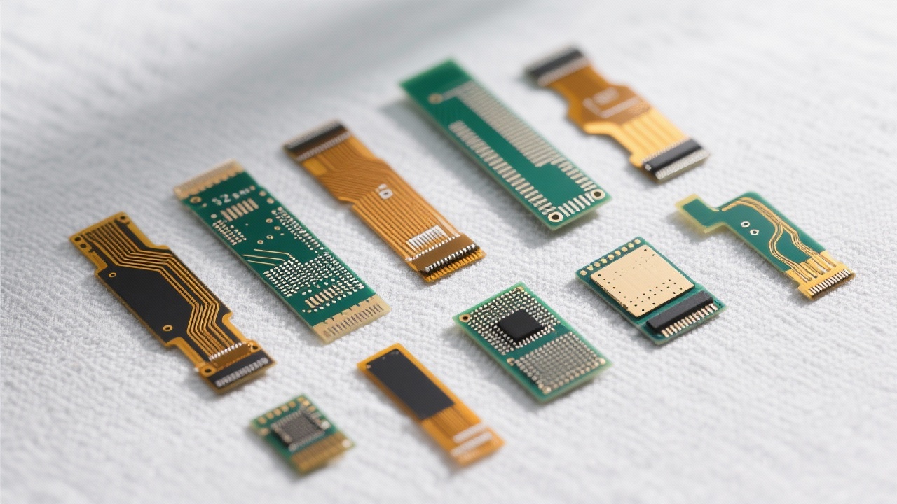
 FPC高密度布线
柔性电路板设计技巧
EMC优化
高密度PCB走线间距
柔性印刷电路制造
305
|
高频PCB阻抗控制
高速多层PCB设计
信号完整性优化
5G基站PCB
高性能介电材料
459
|
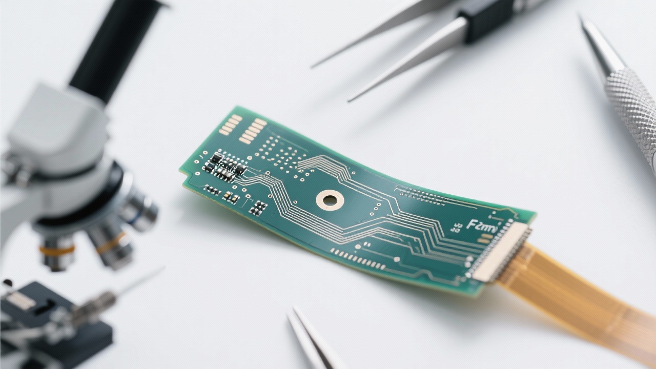
多层FPC过孔设计
FPC弯折应力集中
柔性电路板设计技巧
高密度FPC布线
259
|
阻抗控制
高频PCB
5G基站PCB
信号完整性
高速多层PCB
96
|
FPC高密度布线
柔性电路板设计技术
电磁兼容性优化
高密度柔性PCB
多层FPC制造工艺
FPC高密度布线
柔性电路板设计技巧
EMC优化
高密度PCB走线间距
柔性印刷电路制造
305
|
高频PCB阻抗控制
高速多层PCB设计
信号完整性优化
5G基站PCB
高性能介电材料
459
|
多层FPC过孔设计
FPC弯折应力集中
柔性电路板设计技巧
高密度FPC布线
259
|
阻抗控制
高频PCB
5G基站PCB
信号完整性
高速多层PCB
96
|
FPC高密度布线
柔性电路板设计技术
电磁兼容性优化
高密度柔性PCB
多层FPC制造工艺


-L4-4.png?x-oss-process=image/resize,m_fill,h_800,w_800/format,webp)


-1.png?x-oss-process=image/resize,m_fill,h_800,w_800/format,webp)
