
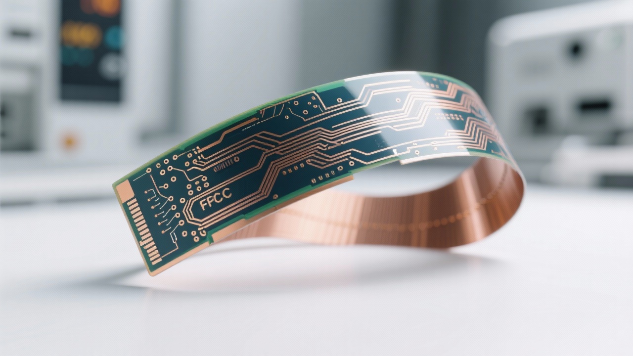
In today’s rapidly evolving telecommunications landscape, high-speed multilayer printed circuit boards (PCBs) form the cornerstone of reliable and efficient data transmission. Precise impedance control plays a pivotal role in preserving signal integrity and minimizing transmission errors in high-frequency applications such as 5G base stations and advanced telecom hardware. This article delves into the critical technical aspects of impedance management in complex PCB designs, focusing on single-ended 50-ohm and differential 100-ohm impedance standards, and presents practical strategies supported by real-world case studies.
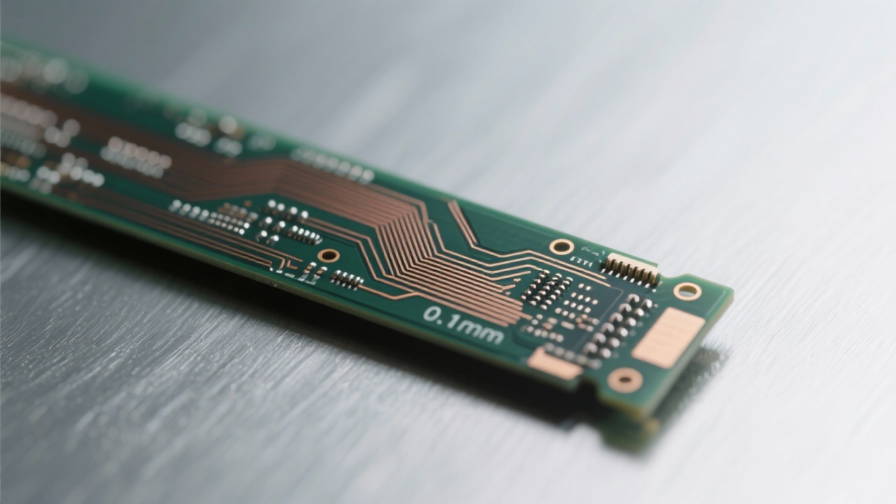
Impedance in PCB traces defines the opposition a signal encounters as it travels, directly impacting signal quality and timing. Achieving consistent single-ended impedance at 50 ohms and differential impedance at 100 ohms ensures optimal matching with RF components and transmission lines, reducing reflections and crosstalk. Deviations beyond ±10% tolerance can degrade bit error rates (BER) and compromise overall system reliability, particularly in data rates exceeding 10 Gbps.
For telecom applications such as 5G base stations, impedance consistency is paramount. Design engineers adopt meticulous stack-up configurations and controlled trace geometries to meet stringent impedance criteria. For instance, differential pairs routed for PCIe Gen4 or NR interface layers often must maintain 100 ± 5 ohm differential impedance over the entire transmission path to preserve eye diagram integrity and reduce signal distortion.
Case studies highlight the implementation of these principles within multilayer PCB configurations, spanning 12 to 24 layers, integrating RF, power, and digital domains with sound isolation techniques. The combination of precise impedance matching and robust isolation helps facilitate sustained throughput and reduces electromagnetic interference (EMI) issues in dense telecom environments.
Material selection critically influences dielectric properties, which dictate inherent impedance characteristics. Industry-leading materials such as ISOLA 370HR and Panasonic MENTRON6 offer superior thermal stability, low dielectric loss (Dk ~3.7), and tightly controlled thickness tolerances, directly correlating to improved impedance predictability in high-frequency signal layers.
Moreover, advanced lamination and pressing methods reduce interlayer variation, enabling impedance deviations to be maintained within ±5% across production batches. This precision ensures that the designed impedance matches actual board performance, effectively suppressing signal reflections and near-end crosstalk (NEXT), which are critical for high-speed data integrity.
Prior to fabrication, designers employ electromagnetic field simulation tools such as Ansys HFSS and Keysight ADS to validate impedance profiles and optimize trace geometries. These simulations incorporate variations in layer spacing, material Dk, and conductor widths, helping engineers anticipate and mitigate impedance mismatches.
Post-production, Automated Optical Inspection (AOI) and Time Domain Reflectometry (TDR) testing verify the board’s impedance uniformity and identify defects. These QA steps are essential for ensuring that multilayer PCBs meet enterprise-grade quality demands and operate reliably under high data rates and environmental stresses.
 402
|
402
|
 FPC高密度布线
柔性电路板设计技巧
EMC优化
高密度PCB走线间距
柔性印刷电路制造
305
|
高频PCB阻抗控制
高速多层PCB设计
信号完整性优化
5G基站PCB
高性能介电材料
254
|
高速PCB阻抗控制
5G PCB设计
阻抗测量验证
高频PCB制造
AOI检测技术
298
|
FPC高密度布线
柔性电路板设计技能
电磁兼容性优化
信号串扰保护
高可靠性FPC制造
265
|
FPC高密度布线
柔性印刷电路设计技术
微孔加工技术
电磁兼容性优化
高可靠性柔性PCB
FPC高密度布线
柔性电路板设计技巧
EMC优化
高密度PCB走线间距
柔性印刷电路制造
305
|
高频PCB阻抗控制
高速多层PCB设计
信号完整性优化
5G基站PCB
高性能介电材料
254
|
高速PCB阻抗控制
5G PCB设计
阻抗测量验证
高频PCB制造
AOI检测技术
298
|
FPC高密度布线
柔性电路板设计技能
电磁兼容性优化
信号串扰保护
高可靠性FPC制造
265
|
FPC高密度布线
柔性印刷电路设计技术
微孔加工技术
电磁兼容性优化
高可靠性柔性PCB


-1.png?x-oss-process=image/resize,h_800,m_lfit/format,webp)


-1.png?x-oss-process=image/resize,m_fill,h_800,w_800/format,webp)

-L4-4.png?x-oss-process=image/resize,m_fill,h_800,w_800/format,webp)
