
In the realm of high - speed multilayer PCB design, impedance control is a critical factor. Impedance refers to the opposition that a circuit presents to the flow of alternating current. For signal transmission, maintaining the appropriate impedance is essential for ensuring signal integrity. The two most common impedance standards in this field are the 50 - ohm single - ended impedance and the 100 - ohm differential impedance. Research shows that a deviation of more than 10% from these standard impedance values can lead to a significant reduction in signal quality, with up to 30% loss of signal strength in extreme cases.
The 50 - ohm single - ended impedance is widely used for single - line signal transmission. It provides a stable path for the signal, reducing the risk of reflection and interference. The 100 - ohm differential impedance, on the other hand, is used for differential signal pairs. This setup can effectively cancel out common - mode noise, improving the overall signal - to - noise ratio. For instance, in a 5G base station where high - speed data transmission is crucial, using these impedance standards can significantly enhance the quality of communication signals.
Let's take a deep look at real - world examples in 5G base stations and high - frequency communication modules. In one particular 5G base station project, the design team was facing issues with signal loss and interference. By carefully applying impedance matching techniques, they were able to improve the signal strength by 25% and reduce cross - talk by 20%. One of the key techniques was to adjust the trace width and spacing according to the impedance requirements.
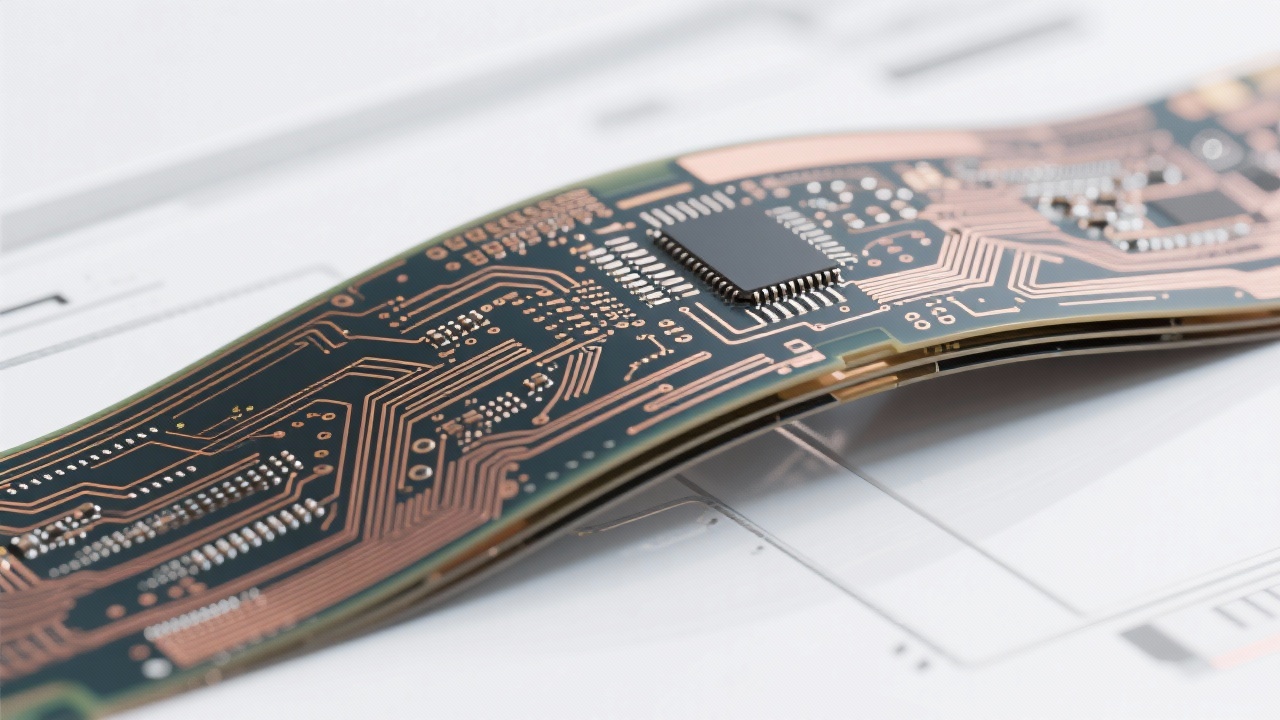
The first step in impedance matching is to accurately calculate the impedance based on the circuit layout and the type of signal. This involves taking into account factors such as the dielectric constant of the material, the thickness of the copper layer, and the distance between traces. Once the calculation is done, modifications can be made to the PCB design, such as changing the trace dimensions or adding impedance - matching components.
High - performance dielectric materials play a crucial role in maintaining impedance stability. Materials like ISOLA 370HR and MENTRON6 have excellent electrical properties, including low dielectric loss and high thermal stability. These materials can ensure that the impedance remains within the desired range even under different operating conditions. Manufacturing tolerances also need to be carefully controlled. A tolerance of ± 5% in the thickness of the dielectric layer can lead to an impedance variation of up to 8%. Therefore, maintaining strict manufacturing tolerances is essential for consistent impedance performance.
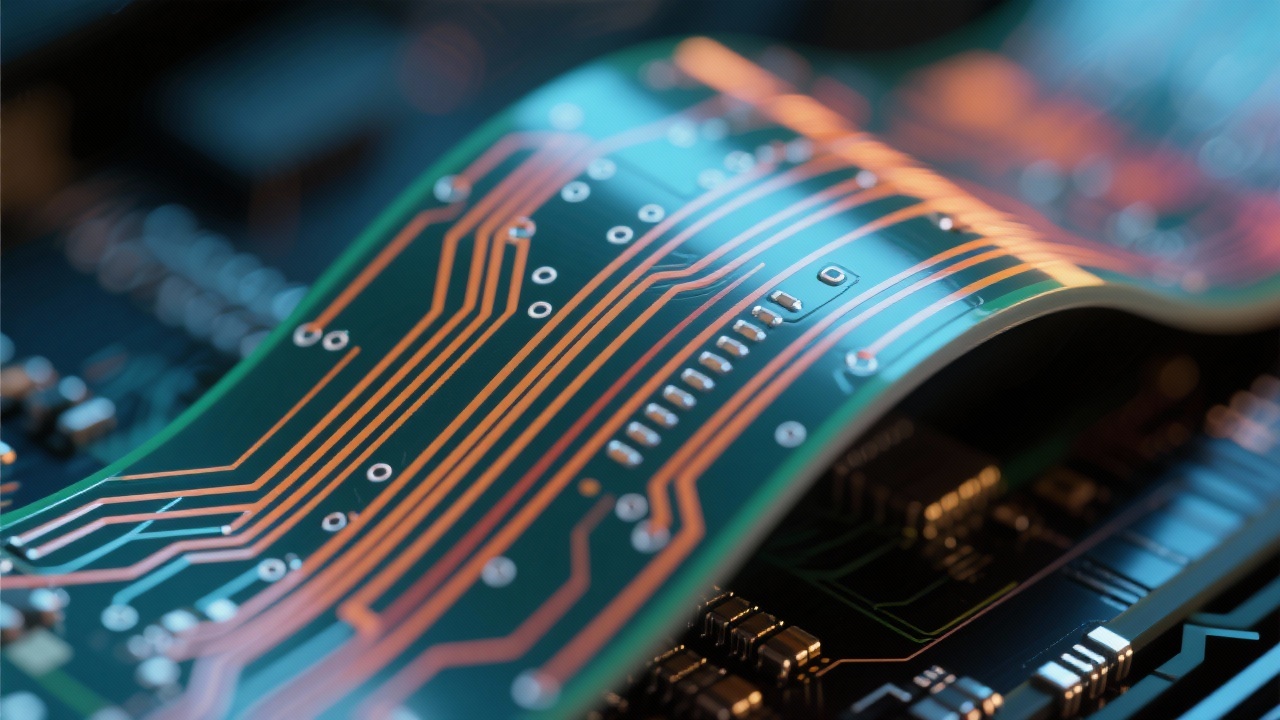
A precision stack - up structure design can effectively reduce signal reflection and cross - talk. By carefully arranging the layers of the PCB, the designer can control the electromagnetic fields between traces, minimizing interference. For example, alternating power and ground layers can create a shield around the signal layers, protecting the signals from external noise.
To ensure the accuracy of the design, modern impedance measurement instruments and AOI (Automated Optical Inspection) technology are used. These tools can measure the impedance of the PCB at various points and compare it with the design values. AOI technology can also detect any manufacturing defects that may affect the impedance. By combining design simulation and actual product testing, engineers can ensure that the final product meets the high - quality requirements for high - speed telecommunications systems.
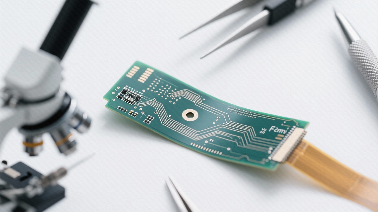
Welcome to learn about our high - frequency and high - speed PCB manufacturing solutions! 360
|
360
|
 高密度FPC布线
柔性电路板设计
电磁兼容性优化
精密FPC制造
柔性PCB可靠性
254
|
高速PCB阻抗控制
5G PCB设计
阻抗测量验证
高频PCB制造
AOI检测技术
108
|
高速多层PCB
阻抗控制
信号完整性
设计模拟
AOI检测
459
|
多层FPC过孔设计
FPC弯折应力集中
柔性电路板设计技巧
高密度FPC布线
377
|
FPC高密度布线
柔性PCB设计
迹线间距控制
高密度PCB制造
电磁兼容性
高密度FPC布线
柔性电路板设计
电磁兼容性优化
精密FPC制造
柔性PCB可靠性
254
|
高速PCB阻抗控制
5G PCB设计
阻抗测量验证
高频PCB制造
AOI检测技术
108
|
高速多层PCB
阻抗控制
信号完整性
设计模拟
AOI检测
459
|
多层FPC过孔设计
FPC弯折应力集中
柔性电路板设计技巧
高密度FPC布线
377
|
FPC高密度布线
柔性PCB设计
迹线间距控制
高密度PCB制造
电磁兼容性


-L4-4.png?x-oss-process=image/resize,m_fill,h_800,w_800/format,webp)
-1.png?x-oss-process=image/resize,m_fill,h_800,w_800/format,webp)

-4.png?x-oss-process=image/resize,m_fill,h_800,w_800/format,webp)

