Why IPC Class 2 PCB Warpage Must Stay Below 0.5% for High-End 34-Layer HDI Boards in Semiconductor Test
2026-02-18
Technical knowledge
This article explains why controlling PCB warpage to ≤0.5% has become a practical benchmark for high-end HDI manufacturing, even though IPC Class 2 allows a higher limit in general use. Focusing on 34-layer HDI boards deployed in semiconductor test platforms, it breaks down how ultra-low warpage directly supports chip placement accuracy, improves SMT solder joint consistency, and stabilizes probe contact repeatability—key factors that influence test yield, maintenance cycles, and overall equipment life. The discussion links warpage performance to core manufacturing and design levers, including balanced multilayer stack-ups (e.g., 1:32:1 symmetry), inner-layer copper thickness compensation strategies, and process stability enabled by advanced German production equipment. With production-proven data examples and clear reference to relevant standards, the article provides engineering-oriented guidance for PCB designers, EMS sourcing teams, and test-system developers, while highlighting the competitive value of achieving ≤0.5% warpage as an industry-recognized quality marker for premium HDI boards.

Why PCB Warpage Must Stay Under 0.5% in High-End HDI Builds (IPC-Class Reality, Not Theory)
PCB warpage is often treated like a cosmetic metric—until it starts breaking yield on a high-layer-count HDI board used in semiconductor test equipment. In that world, warpage is not “acceptable if it passes assembly.” It directly impacts placement accuracy, solder joint integrity, probe contact consistency, and ultimately the stability of the entire test platform.
IPC allows up to 0.75% warpage for many board categories and conditions, yet leading manufacturers and demanding OEMs increasingly require ≤0.5%—especially for complex builds like 34-layer HDI used in testers, handlers, and probe stations. This is not an arbitrary “premium spec.” It is a risk-control threshold learned from production.
What “0.5% Warpage” Actually Means in Manufacturing Terms
Warpage is commonly evaluated as the maximum out-of-plane deviation divided by the board length (or diagonal), expressed as a percentage. A simple numeric example shows why the difference between 0.75% and 0.5% is not small:
| Board Length |
0.75% Max Deviation |
0.5% Max Deviation |
Extra Flatness Gained |
| 200 mm |
1.50 mm |
1.00 mm |
0.50 mm |
| 350 mm |
2.63 mm |
1.75 mm |
0.88 mm |
| 500 mm |
3.75 mm |
2.50 mm |
1.25 mm |
On a large-format tester backplane or multi-board interface assembly, that “extra” millimeter is often the difference between stable probe contact and intermittent open circuits, between smooth SMT and repeated rework cycles.
IPC vs. Real-World HDI: Why 0.5% Became the Unofficial Benchmark
IPC criteria are designed to cover broad product categories and a wide range of use cases. Semiconductor test platforms are not “broad.” They sit at the intersection of high I/O density, tight mechanical tolerances, and repetitive contact stress (probing cycles). In practice, OEMs and EMS providers tighten the requirement to reduce hidden costs:
1) SMT yield is more sensitive than the spec implies
Fine-pitch BGAs, LGA packages, and HDI escape routing rely on consistent coplanarity. When the PCB bows, the stencil-to-pad contact changes, paste volume varies, and the reflow process produces uneven wetting. Even if assembly “passes,” latent defects become more likely under thermal cycling.
2) Probe contact stability is unforgiving
Semiconductor test fixtures depend on consistent normal force and alignment across hundreds or thousands of contact points. Excessive warpage alters contact force distribution, driving up contact resistance variance. The result is noise, false fails, and repeated test cycles—problems that look like “software” until someone measures flatness.
3) Mechanical stress accumulates over time
A tester can see frequent board insertions/removals, localized heating, and sustained clamping. Warpage accelerates connector wear, increases micro-motion at solder joints, and amplifies stress around via structures. A tighter warpage target acts as a reliability multiplier.
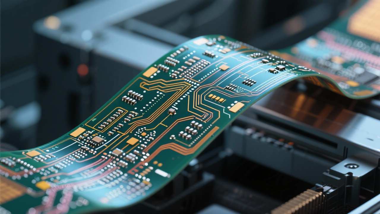
The Hidden Drivers of Warpage in 34-Layer HDI (And What Actually Works)
Warpage is not a single-variable defect. For a 34-layer HDI stackup, it is a cumulative result of material behavior, copper distribution, lamination symmetry, and process discipline. Teams that reliably reach ≤0.5% do not rely on one trick—they build a system.
Stackup symmetry: it’s not “nice to have”
A common high-layer-count approach is to maintain mirror symmetry across the centerline (for example, a concept similar to 1:32:1 balancing principles—outer layers and build-up structures mirrored). When dielectric thickness and copper weights are balanced, thermal expansion and resin shrinkage are less likely to pull the panel into a bow or twist.
Copper thickness compensation: the “silent lever” for flatness
In 34-layer designs, inner-layer copper thickness can vary due to pattern density, plating behavior, and etch-back effects. If copper distribution is not actively compensated, lamination becomes mechanically biased. In production, leading HDI factories apply a controlled methodology:
- Inner-layer copper balancing using thieving, copper pour strategy, and density rules to reduce local stress gradients.
- Targeted copper weight planning (e.g., 0.5 oz to 1 oz equivalents on specific layers) to keep the stack’s neutral axis stable.
- Plating uniformity control to reduce side-to-side thickness deviations that convert into twist after lamination.
The practical goal is simple: when the board comes out of press and sees reflow temperatures, it should “want” to remain flat, not fight the fixture.
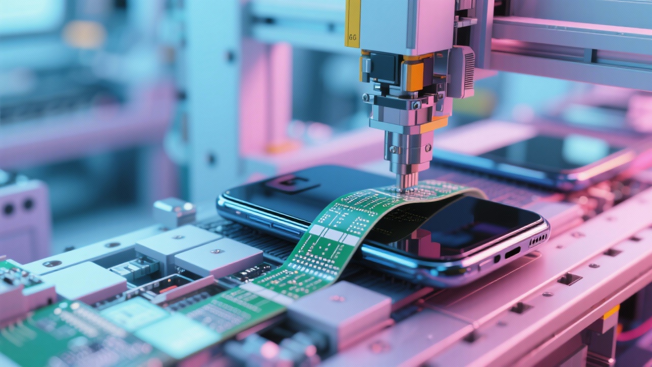
How Advanced German Equipment Supports the 0.5% Warpage Target
Process capability matters as much as design intent. High-end lines built around German-origin process equipment (commonly in drilling, imaging, lamination control, and AOI/metrology ecosystems) reduce warpage not by “magic,” but by reducing variation. Lower variation means fewer hidden stress imbalances.
Where equipment-level control makes a measurable difference
Press temperature/pressure uniformity: tighter thermal gradients reduce resin flow imbalances that “lock in” curvature after cooling.
Registration and imaging stability: accurate alignment lowers the need for aggressive rework or compensation that can create uneven copper density.
Metrology feedback loops: when warpage and thickness are measured consistently, process windows can be narrowed with real SPC, not assumptions.
Production Data Snapshot: What Changes When Warpage Drops Below 0.5%
In high-mix manufacturing, “warpage control” must prove itself in yield, reliability, and field stability. The following reference ranges are typical of what EMS and test-equipment OEMs report when moving from a looser control band (near the IPC limit) to a tighter ≤0.5% control target on complex HDI builds:
| Metric (Typical for HDI Assemblies) |
Near 0.75% Warpage |
≤0.5% Warpage |
Operational Impact |
| SMT first-pass yield (fine-pitch + large PCB) |
96.5%–98.0% |
98.8%–99.5% |
Fewer touch-ups, less hidden reliability risk |
| BGA open/HiP defect rate (per 10k joints) |
35–60 |
10–25 |
Improved coplanarity and paste transfer consistency |
| Probe contact instability (retest rate) |
1.2%–2.0% |
0.3%–0.8% |
Fewer false fails, higher throughput |
| Fixture wear / maintenance interval (relative) |
Baseline |
+15% to +30% |
Lower uneven loading across contact points |
These gains are the reason the market treats 0.5% as a practical threshold: it reduces systemic variation, and systemic variation is what makes high-end testers unpredictable.
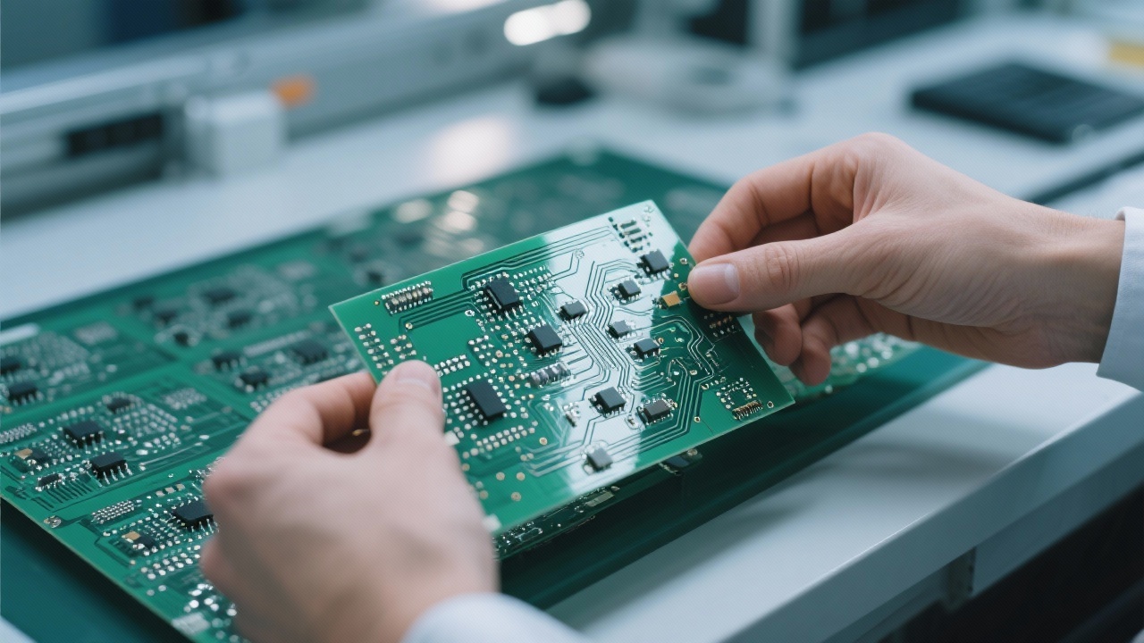
What EMS Buyers and Test-Platform Engineers Should Ask for (Beyond a Warpage Number)
A warpage promise without process transparency is just a number on a drawing. When qualifying a high-end HDI supplier for semiconductor test applications, experienced teams commonly request evidence that the factory can repeat the result across lots:
- Lot-to-lot warpage data with sample size, measurement method, and board condition (as fabricated vs. post-reflow simulation).
- Stackup symmetry documentation and controlled dielectric/copper tolerance targets.
- Copper distribution strategy (how the supplier manages density and plating uniformity on internal layers).
- SPC controls on lamination parameters and thickness uniformity.
- Application awareness: supplier understands probe stability, connector loading, and large-format assembly constraints.
CTA: If Your Test Hardware Can’t Tolerate Drift, Don’t Let Warpage Be the Variable
Request a Warpage-Control Plan for 34-Layer HDI PCB Builds to the ≤0.5% Benchmark
For semiconductor test equipment, the best time to control warpage is before the first lamination cycle—through stackup symmetry, copper compensation, and repeatable process windows. A qualified HDI partner should be able to share measurement methods, typical lot data, and the exact controls used to keep large panels flat.
Talk to an Engineer About Low-Warpage 34-Layer HDI PCB Manufacturing
Typical response time: 1 business day. Share your outline drawing, panel size, stackup intent, and assembly constraints to get a practical recommendation.
When a 34-layer HDI board is built for semiconductor test, the question is rarely whether the PCB can be made—it is whether it can remain mechanically predictable through assembly, probing cycles, and uptime demands where every micron of deflection can quietly become a retest, a false fail, or a maintenance event.


-L4-4.png?x-oss-process=image/resize,m_fill,h_800,w_800/format,webp)


-4.png?x-oss-process=image/resize,m_fill,h_800,w_800/format,webp)


