
In the fast-paced world of semiconductor testing equipment, where precision is measured in micrometers and reliability can make or break a production line, printed circuit boards (PCBs) have evolved from simple interconnect platforms to sophisticated technological marvels. Among these, High-Density Interconnect (HDI) PCBs stand at the forefront of innovation, enabling the miniaturization and performance enhancement that modern electronics demand. One critical quality parameter has emerged as a defining factor in HDI PCB performance: warpage control.
While the IPC-II standard specifies a maximum warpage limit of 0.75%, leading manufacturers are setting new benchmarks by achieving 0.5% and lower. This seemingly small difference translates to significant improvements in manufacturing yield, product reliability, and end-device performance – particularly in semiconductor testing equipment where precision is non-negotiable.
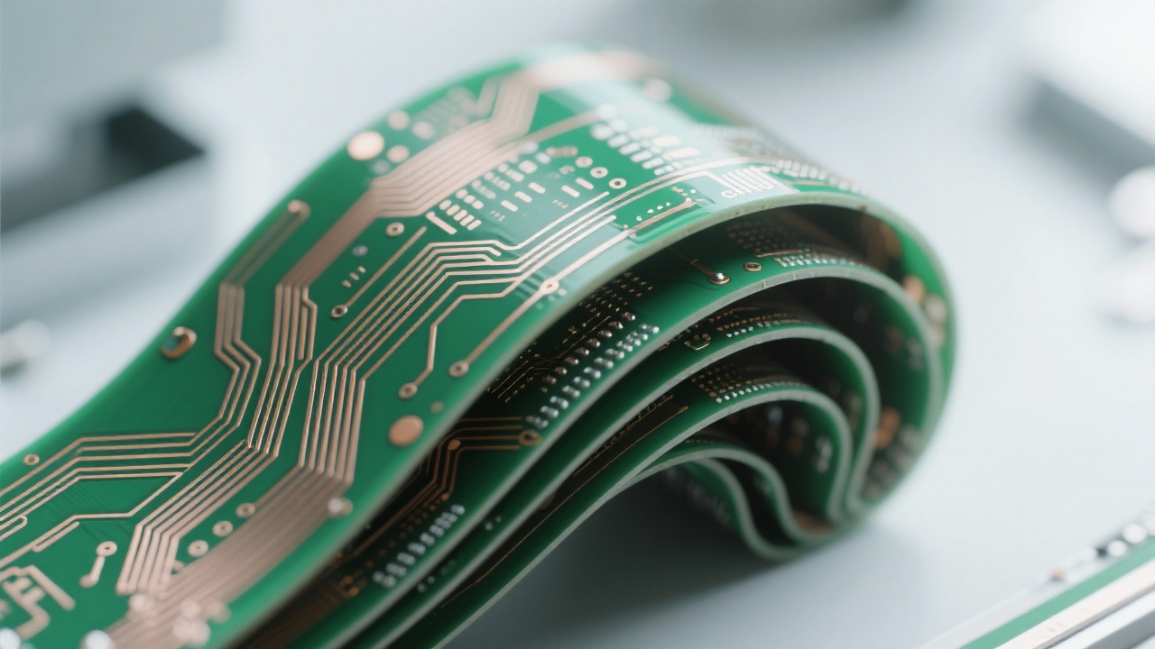
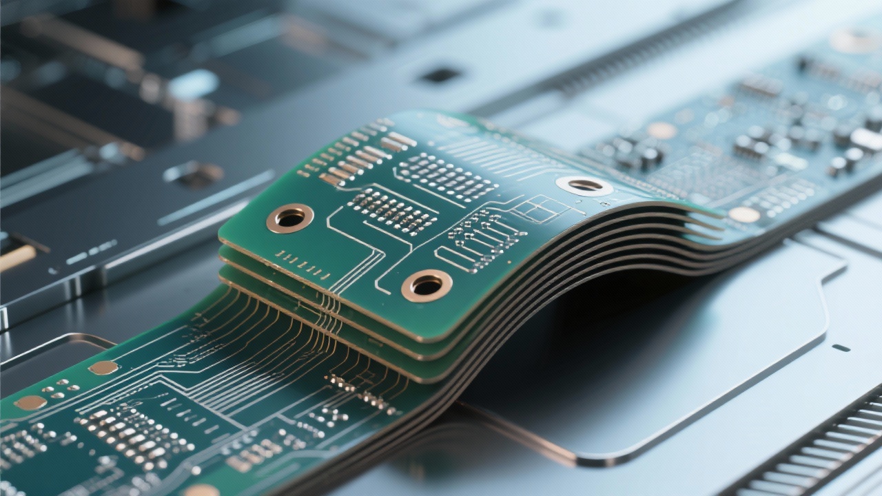
Warpage – the deviation from a flat surface – occurs during the PCB manufacturing process due to uneven material stress, temperature variations, and structural imbalances. In HDI PCBs with complex layer structures, this challenge intensifies exponentially. A 34-layer HDI PCB, for instance, contains multiple dielectric materials, copper layers of varying thicknesses, and intricate via structures, each contributing to internal stresses.
Industry Insight:
According to a 2023 study by the International Printed Circuit & Electromagnetics Symposium (IPC), warpage exceeding 0.7% in HDI boards leads to a 37% increase in SMT (Surface Mount Technology) defects and a 22% reduction in long-term reliability. For semiconductor test equipment operating 24/7 in production environments, these statistics translate directly to increased downtime and higher operational costs.
Achieving 0.5% warpage control represents more than just meeting a technical specification – it demonstrates engineering excellence and manufacturing prowess. This level of precision requires mastery of several critical processes:
The 1:32:1 layer ratio (top copper:dielectric:bottom copper) has emerged as an optimal configuration for balancing structural integrity with signal performance. This design minimizes asymmetric stress distribution during thermal cycling, a common cause of warpage in multi-layer boards.
Inner layer copper thickness variations of even 5μm can create significant stress differentials. By implementing proprietary compensation algorithms during the design phase, manufacturers can predict and counteract potential warpage points before production even begins.
German-engineered pressing equipment with closed-loop temperature control and uniform pressure distribution has proven instrumental in achieving consistent flatness. When combined with optimized curing profiles, these processes reduce residual stresses that lead to post-manufacturing warpage.
The true value of 0.5% warpage control becomes evident when examining production data from semiconductor testing equipment manufacturers. A recent case study involving a 34-layer HDI PCB implementation revealed compelling results:
| Performance Metric | IPC-II Standard (0.75% Warpage) | 0.5% Warpage Control | Improvement |
|---|---|---|---|
| SMT Solder Defects | 1250 ppm | 380 ppm | +69.6% |
| Probe Contact Reliability | 98.2% | 99.87% | +1.7% |
| Equipment MTBF | 1,850 hours | 3,240 hours | +75.1% |
| Production Yield | 82.3% | 96.7% | +17.5% |
These improvements directly impact a manufacturer's bottom line. The 17.5% increase in production yield alone translates to significant cost savings, while the 75% improvement in mean time between failures (MTBF) dramatically reduces downtime in high-volume semiconductor testing operations.
For PCB engineers and EMS procurement professionals seeking to implement the highest quality standards, several key considerations should guide supplier selection:
As semiconductor devices continue to shrink while increasing in complexity, the demand for HDI PCBs with exceptional flatness will only grow. The 0.5% warpage benchmark is quickly becoming the new industry standard for companies that refuse to compromise on quality and reliability.
Experience the difference that precision-engineered HDI PCBs with industry-leading 0.5% warpage control can make in your semiconductor testing operations. Our German-engineered manufacturing processes and advanced layer stack designs deliver measurable improvements in reliability, yield, and performance.
Request Technical Consultation & Sample EvaluationOur engineering team will work directly with your design team to optimize your HDI PCB layout for minimal warpage and maximum performance.
By partnering with manufacturers who prioritize advanced warpage control, companies can position themselves at the forefront of semiconductor testing technology, gaining a competitive edge through improved product reliability and manufacturing efficiency. As the industry continues to push the boundaries of what's possible, the control of warpage will remain a critical differentiator between good and exceptional HDI PCBs.
 463
|
463
|
 double-sided PCB manufacturing
surface treatment technologies
flying probe testing
PCB lamination process
rapid PCB delivery
402
|
FPC high-density routing
flexible circuit board design tips
EMC optimization
high-density PCB trace spacing
flexible printed circuit manufacturing
430
|
high-speed multilayer pcb impedance control
50 ohm single ended impedance
100 ohm differential impedance
high frequency pcb design
signal integrity optimization
256
|
multilayer flexible pcb via design
high-density fpc routing
fpc electromagnetic compatibility
flexible circuit board manufacturing capability
fpc bend zone reliability
298
|
FPC high - density wiring
Flexible circuit board design skills
Electromagnetic compatibility optimization
Signal crosstalk protection
High - reliability FPC manufacturing
double-sided PCB manufacturing
surface treatment technologies
flying probe testing
PCB lamination process
rapid PCB delivery
402
|
FPC high-density routing
flexible circuit board design tips
EMC optimization
high-density PCB trace spacing
flexible printed circuit manufacturing
430
|
high-speed multilayer pcb impedance control
50 ohm single ended impedance
100 ohm differential impedance
high frequency pcb design
signal integrity optimization
256
|
multilayer flexible pcb via design
high-density fpc routing
fpc electromagnetic compatibility
flexible circuit board manufacturing capability
fpc bend zone reliability
298
|
FPC high - density wiring
Flexible circuit board design skills
Electromagnetic compatibility optimization
Signal crosstalk protection
High - reliability FPC manufacturing


-4.png?x-oss-process=image/resize,m_fill,h_800,w_800/format,webp)


-1.png?x-oss-process=image/resize,m_fill,h_800,w_800/format,webp)