
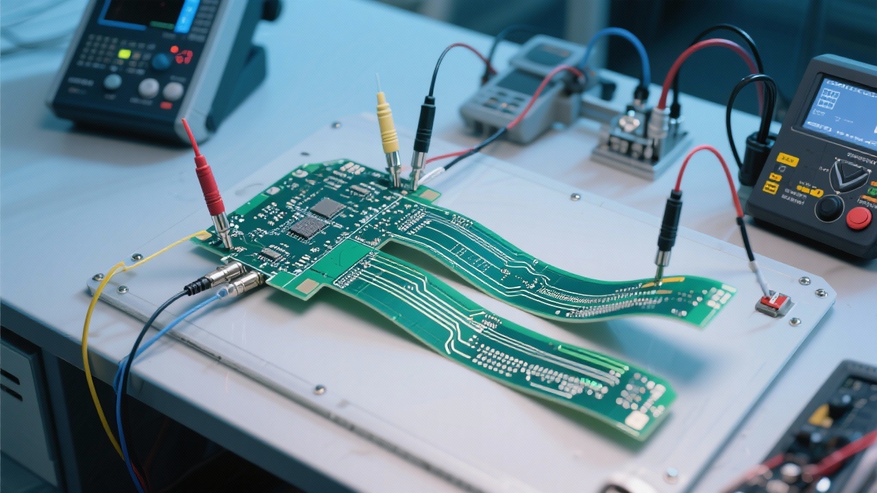
In the era of 5G and high-frequency communications, the integrity of signals within multilayer printed circuit boards (PCBs) has become paramount. One of the critical factors influencing signal quality is the impedance stability. This industry-focused research explores how advanced dielectric substrates like ISOLA 370HR and Panasonic MENTRON6 in conjunction with precise manufacturing tolerances enable reliable impedance control, essential for achieving optimal signal performance in high-speed applications.
Impedance control is fundamental in minimizing signal reflection and crosstalk within complex multilayer PCBs used in modern telecommunication systems, especially 5G base stations. Typically, these designs adhere to standardized impedance targets—50Ω single-ended and 100Ω differential impedances—ensuring standardized signal environments for integrated circuits and transmission lines. Deviations as small as ±5% can lead to significant signal degradation and increased electromagnetic interference.
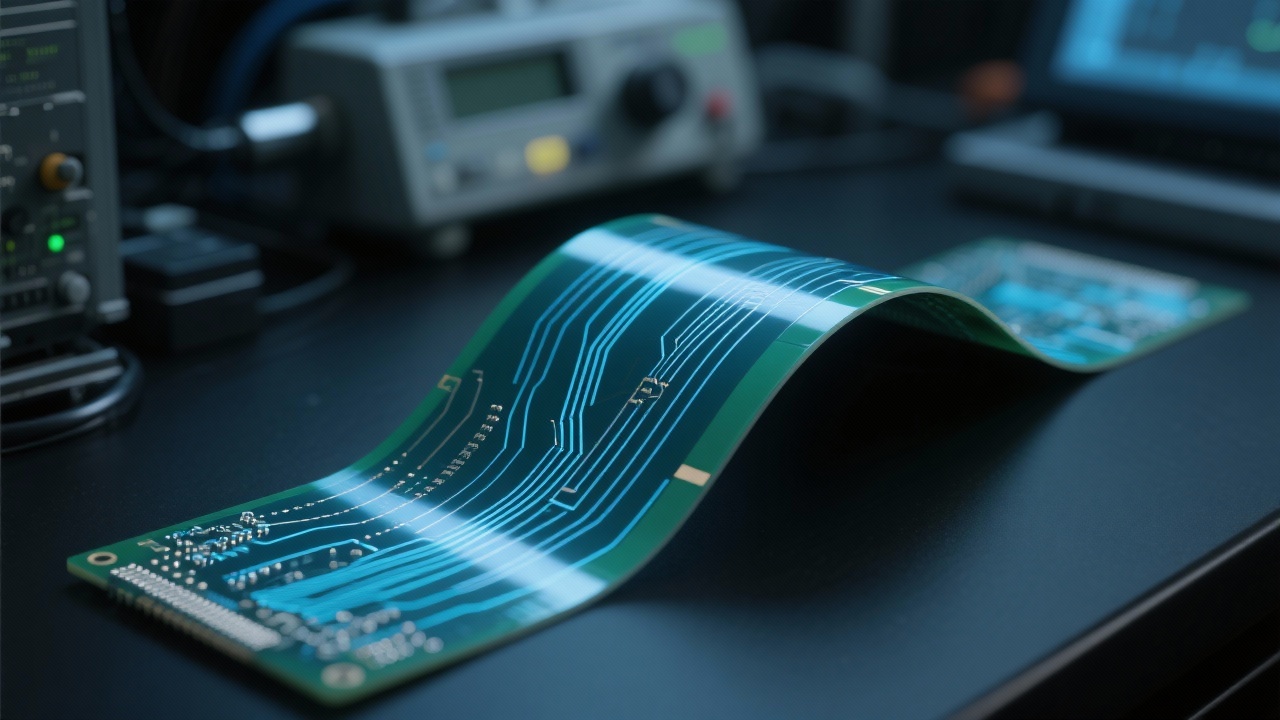
High-performance dielectric materials like ISOLA 370HR and Panasonic MENTRON6 offer low dielectric loss (Dk ~3.7 to 4.0) and consistent dielectric constants, which are crucial for signal integrity at frequencies beyond 10 GHz. The multilayer stackup—including prepreg layers, core thicknesses, and copper foil—must be meticulously designed to maintain a stable characteristic impedance throughout the board.
Such stackups must maintain key dimensional parameters within tight tolerances: prepreg thickness variations under ±5 μm and copper foil thickness around 18 μm (0.7 mils) with less than ±10% variation. These factors collectively stabilize the effective dielectric constant and impedance.
Manufacturing precision is as vital as material selection. Typical process tolerances include:
Quality assurance employs sophisticated simulation tools alongside Automated Optical Inspection (AOI) to validate impedance and detect manufacturing defects. For example, time-domain reflectometry (TDR) simulations predict expected impedance profiles, while AOI verifies line width and spacing adherence to specifications. Coupling these techniques enables a robust end-to-end impedance control workflow.
Beyond materials and process control, adhering to international certifications such as IPC-6012 for high-frequency PCB manufacturing ensures a standardized quality baseline. Collaborations between material suppliers, PCB fabricators, and design engineers are pivotal in tuning the design-to-manufacture loop for impedance stability.
By integrating these strategies—informed material selection, rigorous tolerance adherence (e.g., 3-mil line widths and 5 μ" ENIG surface finishes), and advanced testing—manufacturers can achieve multilayer PCBs that excel in signal integrity and reliability required for 5G and future high-speed communication infrastructure.
 419
|
419
|
 FPC高密度布线
柔性PCB设计技术
电磁干扰优化
信号串扰抑制
柔性PCB制造工艺
412
|
双层PCB快速制造
PCB工艺流程
表面处理技术
飞针测试
PCB可靠性检测
459
|
多层FPC过孔设计
FPC弯折应力集中
柔性电路板设计技巧
高密度FPC布线
317
|
高密度FPC布线
柔性PCB设计
电磁干扰优化
医疗 FPC
消费电子产品FPC
259
|
阻抗控制
高频PCB
5G基站PCB
信号完整性
高速多层PCB
FPC高密度布线
柔性PCB设计技术
电磁干扰优化
信号串扰抑制
柔性PCB制造工艺
412
|
双层PCB快速制造
PCB工艺流程
表面处理技术
飞针测试
PCB可靠性检测
459
|
多层FPC过孔设计
FPC弯折应力集中
柔性电路板设计技巧
高密度FPC布线
317
|
高密度FPC布线
柔性PCB设计
电磁干扰优化
医疗 FPC
消费电子产品FPC
259
|
阻抗控制
高频PCB
5G基站PCB
信号完整性
高速多层PCB


-1.png?x-oss-process=image/resize,m_fill,h_800,w_800/format,webp)


-4.png?x-oss-process=image/resize,h_800,m_lfit/format,webp)

-1.png?x-oss-process=image/resize,h_800,m_lfit/format,webp)


